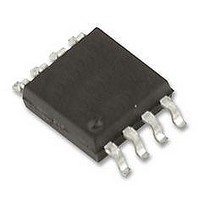
LT1999MPMS8-10#PBF Linear Technology, LT1999MPMS8-10#PBF Datasheet - Page 16

LT1999MPMS8-10#PBF
Manufacturer Part Number
LT1999MPMS8-10#PBF
Description
SC-Amps/Current Sense, High Voltage, Bidirectional Current Sense Amplifier
Manufacturer
Linear Technology
Datasheet
1.LT1999MPMS8-10PBF.pdf
(24 pages)
Specifications of LT1999MPMS8-10#PBF
Input Bias Current
137.5µA
Output Current Per Channel
26mA
Input Offset Voltage
1.5mV
Bandwidth
2MHz
Cmrr
120dB
Slew Rate
3V/µs
Supply Voltage Range
4.5V To 5.5V
Supply Current
3µA
Rohs Compliant
Yes
No. Of Amplifiers
2
Available stocks
Company
Part Number
Manufacturer
Quantity
Price
APPLICATIONS INFORMATION
LT1999-10/LT1999-20/
LT1999-50
Shutdown Capability
If SHDN (Pin 8) is driven to within 0.5V of GND, the LT1999
is placed into a low power shutdown state in which the
part will draw about 3μA from the V
pins (+IN and –IN) will draw approximately 1nA if biased
within the range of 0V to 80V (with no differential voltage
applied). If the input pins are pulled below the GND pin,
each input appears as a diode tied to GND in series with
approximately 4k of resistance. The REF pin appears as
approximately 0.4MΩ tied to a mid-supply potential. The
output appears as reverse biased diodes tied between the
output to either V
EMI Filtering and Layout Practices
An internal 1st order differential lowpass noise/EMI sup-
pression fi lter with a –3dB bandwidth of 10MHz (approxi-
mately 5× the LT1999’s –3dB bandwidth) is included to
help improve the LT1999’s EMI susceptibility and to assist
with the rejection of high frequency signals beyond the
16
+
or GND pins.
FROM DC SOURCE
TO LOAD
+
* KEEP LOOP AREA COMPRISING R
** REF BYPASS TIED TO A LOW NOISE, LOW IMPEDANCE
† OPTIONAL 10pF CAPACITOR TO PREVENT dV/dt EDGES
supply. The input
AS SMALL AS POSSIBLE.
SIGNAL GROUND PLANE.
ON INPUT COUPLING TO FLOATING SHDN PIN.
R
SENSE
Figure 4. Recommended Layout
*
1
2
3
4
SUPPLY BYPASS
V
+IN
–IN
V
†
+
+
CAPACITOR
bandwidth of the LT1999 that may introduce errors. The
pole is set by the following equation:
Both the resistors and capacitors have a ±15% variation
so the pole can vary by approximately ±30% over manu-
facturing process and temperature variations.
The layout for lowest EMI/noise susceptibility is achieved
by keeping short direct connections and minimizing loop
areas (see Figure 4). If the user-supplied sense resistor
cannot be placed in close proximity to the LT1999, the
surface area of the loop comprising connections of +IN
to R
quires routing PCB traces connecting +IN to R
–IN to R
separation. The metal traces connecting +IN to the sense
resistor and –IN to the sense resistor should match and
use the same trace width.
Bypassing the V
with short wiring connection is recommended.
SENSE
f
fi lt
SENSE
SHDN
, +IN AND –IN PINS
GND
OUT
REF
= 1/(π•(R
SENSE
8
7
6
5
and back to –IN should be minimized. This re-
adjacent with one another with minimal
+
+ IN
pin to the GND pin with a 0.1μF capacitor
1999 F03
**
+ R
DIFFERENTIAL
ANALOG OUT
– IN
)•C
F
) ≈ 10MHz
SENSE
1999fa
and


