BAV99,235 NXP Semiconductors, BAV99,235 Datasheet
BAV99,235
Specifications of BAV99,235
933215370235
BAV99 /T3
BAV99 /T3
BAV99,235
Available stocks


Related parts for BAV99,235


BAV99,235 Summary of contents
Page 1
BAV99 series High-speed switching diodes Rev. 8 — 18 November 2010 1. Product profile 1.1 General description High-speed switching diodes, encapsulated in small Surface-Mounted Device (SMD) plastic packages. Table 1. Type number BAV99 BAV99S BAV99W 1.2 Features and benefits High ...
Page 2
... NXP Semiconductors 2. Pinning information Table 3. Pin BAV99; BAV99W BAV99S Ordering information Table 4. Type number BAV99 BAV99S BAV99W 4. Marking Table 5. Type number BAV99 BAV99S BAV99W [ placeholder for manufacturing site code BAV99_SER Product data sheet Pinning Description anode (diode 1) cathode (diode 2) cathode (diode 1), ...
Page 3
... NXP Semiconductors 5. Limiting values Table 6. In accordance with the Absolute Maximum Rating System (IEC 60134). Symbol Per diode V RRM FRM I FSM P tot Per device amb T stg [1] Single diode loaded. [2] Double diode loaded °C prior to surge. [ [4] Device mounted on an FR4 Printed-Circuit Board (PCB), single-sided copper, tin-plated and standard footprint ...
Page 4
... NXP Semiconductors 6. Thermal characteristics Table 7. Symbol R th(j-a) R th(j-sp) [1] Single diode loaded. [2] Device mounted on an FR4 PCB, single-sided copper, tin-plated and standard footprint. [3] Soldering points at pins and 6. 7. Characteristics Table amb Symbol Per diode [1] When switched from I [2] When switched from I BAV99_SER ...
Page 5
... NXP Semiconductors (mA (1) (2) (3) 1 − 0.2 0.4 0.6 0.8 = 150 °C (1) T amb = 85 °C (2) T amb = 25 °C (3) T amb = −40 °C (4) T amb Fig 1. Forward current as a function of forward voltage; typical values 0 (pF ) 0.6 0.4 0 ° MHz; T amb Fig 3. Diode capacitance as a function of reverse voltage ...
Page 6
... NXP Semiconductors 8. Test information D.U. Ω × ( Input signal: reverse pulse rise time t Oscilloscope: rise time Fig 5. Reverse recovery time test circuit and waveforms I 450 Ω 1 kΩ Ω D.U.T. Input signal: forward pulse rise time t Fig 6. Forward recovery voltage test circuit and waveforms 8 ...
Page 7
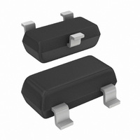
... NXP Semiconductors 9. Package outline 3.0 2.8 3 2.5 1.4 2.1 1.2 1 1.9 Dimensions in mm Fig 7. Package outline BAV99 (SOT23/TO-236AB) Fig 9. Package outline BAV99W (SOT323/SC-70) 10. Packing information Table 9. The indicated -xxx are the last three digits of the 12NC ordering code. Type number Package ...
Page 8
... NXP Semiconductors 11. Soldering 3 1.7 Fig 10. Reflow soldering footprint BAV99 (SOT23/TO-236AB) 2.6 4.6 Fig 11. Wave soldering footprint BAV99 (SOT23/TO-236AB) BAV99_SER Product data sheet 3.3 2.9 1.9 0.7 (3×) 0.5 (3×) 0.6 (3×) 1 2.2 1.2 (2×) 1.4 (2×) 1.4 2.8 4.5 All information provided in this document is subject to legal disclaimers. ...
Page 9
... NXP Semiconductors Fig 12. Reflow soldering footprint BAV99S (SOT363/SC-88) 4.5 Fig 13. Wave soldering footprint BAV99S (SOT363/SC-88) BAV99_SER Product data sheet 2.65 2.35 1.5 0.6 0.5 (4×) (4×) 0.5 (4×) 0.6 (4×) 1.8 1.3 1.3 2.45 5.3 All information provided in this document is subject to legal disclaimers. ...
Page 10
... NXP Semiconductors Fig 14. Reflow soldering footprint BAV99W (SOT323/SC-70) 3.65 2.1 Fig 15. Wave soldering footprint BAV99W (SOT323/SC-70) BAV99_SER Product data sheet 2.65 1.85 1.325 2 0.6 3 2.35 (3×) 1 0.55 (3×) 4.6 2.575 1.425 (3×) All information provided in this document is subject to legal disclaimers. Rev. 8 — 18 November 2010 ...
Page 11
... NXP Semiconductors 12. Revision history Table 10. Revision history Document ID Release date BAV99_SER_8 20101118 • Modifications: Section 4 • Section 5 “Limiting • Section 13 “Legal BAV99_SER_7 20100414 BAV99_SER_6 20100310 BAV99_SER_5 20080820 BAV99_4 20011015 BAV99S_3 20010514 BAV99W_4 19990511 BAV99_SER Product data sheet Data sheet status Product data sheet “ ...
Page 12
... In no event shall NXP Semiconductors be liable for any indirect, incidental, punitive, special or consequential damages (including - without limitation - lost profits, lost savings, business interruption, costs related to the removal or ...
Page 13
... NXP Semiconductors Quick reference data — The Quick reference data is an extract of the product data given in the Limiting values and Characteristics sections of this document, and as such is not complete, exhaustive or legally binding. 14. Contact information For more information, please visit: For sales office addresses, please send an email to: ...
Page 14
... NXP Semiconductors 15. Contents 1 Product profile . . . . . . . . . . . . . . . . . . . . . . . . . . 1 1.1 General description . . . . . . . . . . . . . . . . . . . . . 1 1.2 Features and benefits . . . . . . . . . . . . . . . . . . . . 1 1.3 Applications . . . . . . . . . . . . . . . . . . . . . . . . . . . 1 1.4 Quick reference data . . . . . . . . . . . . . . . . . . . . 1 2 Pinning information . . . . . . . . . . . . . . . . . . . . . . 2 3 Ordering information . . . . . . . . . . . . . . . . . . . . . 2 4 Marking . . . . . . . . . . . . . . . . . . . . . . . . . . . . . . . . 2 5 Limiting values Thermal characteristics . . . . . . . . . . . . . . . . . . 4 7 Characteristics . . . . . . . . . . . . . . . . . . . . . . . . . . 4 8 Test information . . . . . . . . . . . . . . . . . . . . . . . . . 6 8.1 Quality information . . . . . . . . . . . . . . . . . . . . . . 6 9 Package outline . . . . . . . . . . . . . . . . . . . . . . . . . 7 10 Packing information ...