MURD620CTG ON Semiconductor, MURD620CTG Datasheet
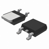
DIODE ULTRA FAST 200V 3A DPAK

MURD620CTG

Manufacturer Part Number
MURD620CTG
Description
DIODE ULTRA FAST 200V 3A DPAK
Manufacturer
ON Semiconductor
Series
SWITCHMODE™r
Datasheet

Specifications of MURD620CTG

Voltage - Forward (vf) (max) @ If
1V @ 3A
Current - Reverse Leakage @ Vr
5µA @ 200V
Current - Average Rectified (io) (per Diode)
3A
Voltage - Dc Reverse (vr) (max)
200V
Reverse Recovery Time (trr)
35ns
Diode Type
Standard
Speed
Fast Recovery =< 500ns, > 200mA (Io)
Diode Configuration
1 Pair Common Cathode
Mounting Type
Surface Mount
Package / Case
DPak, TO-252 (2 leads+tab), SC-63
Rectifier Type
Switching Diode
Configuration
Dual Common Cathode
Peak Rep Rev Volt
200V
Avg. Forward Curr (max)
6A
Rev Curr
5uA
Peak Non-repetitive Surge Current (max)
50A
Forward Voltage
1.2V
Operating Temp Range
-65C to 175C
Package Type
DPAK
Rev Recov Time
35ns
Operating Temperature Classification
Military
Mounting
Surface Mount
Pin Count
2 +Tab
Lead Free Status / RoHS Status
Lead free / RoHS Compliant

Available stocks

Company
Part Number
Manufacturer
Quantity
Price
Part Number:
MURD620CTG
Manufacturer:
ON Semiconductor
Quantity:
1 608
Part Number:
MURD620CTG
Manufacturer:
ON
Quantity:
12 500
MURD620CT
SWITCHMODE
Power Rectifier
DPAK Surface Mount Package
power supplies, inverters and as free wheeling diodes.
Features
Mechanical Characteristics:
Stresses exceeding Maximum Ratings may damage the device. Maximum
Ratings are stress ratings only. Functional operation above the Recommended
Operating Conditions is not implied. Extended exposure to stresses above the
Recommended Operating Conditions may affect device reliability.
1. Rating applies when surface mounted on the minimum pad sizes
MAXIMUM RATINGS
THERMAL CHARACTERISTICS
© Semiconductor Components Industries, LLC, 2011
January, 2011 − Rev. 9
Peak Repetitive Reverse Voltage
Working Peak Reverse Voltage
DC Blocking Voltage
Average Rectified Forward Current
(Rated V
Peak Repetitive Forward Current
(Rated V
20 kHz, T
Non−Repetitive Peak Surge Current
(Surge Applied at Rated Load Conditions
Halfwave, 60 Hz)
Operating Junction and Storage
Temperature Range
Thermal Resistance, Junction−to−Case
Thermal Resistance, Junction−to−Ambient
(Note 1)
These state−of−the−art devices are designed for use in switching
Leads are Readily Solderable
260°C Max. for 10 Seconds
Ultrafast 35 Nanosecond Recovery Time
Low Forward Voltage Drop
Low Leakage
Pb−Free Packages are Available
Case: Epoxy, Molded
Weight: 0.4 Gram (Approximately)
Finish: All External Surfaces Corrosion Resistant and Terminal
Lead and Mounting Surface Temperature for Soldering Purposes:
recommended.
R
R
, T
C
, Square Wave,
= 145°C)
C
= 140°C)
Rating
Rating
Per Device
Per Diode
Per Diode
(Per Diode)
Symbol
Symbol
T
V
V
I
R
I
R
J
F(AV)
FSM
RWM
V
RRM
, T
I
qJC
qJA
F
R
stg
−65 to +175
Value
Value
200
3.0
6.0
6.0
50
80
9
1
°C/W
°C/W
Unit
Unit
°C
V
A
A
A
†For information on tape and reel specifications,
MURD620CT
MURD620CTT4
MURD620CTT4G
MURD620CTG
1 2
including part orientation and tape sizes, please
refer to our Tape and Reel Packaging Specifications
Brochure, BRD8011/D.
Device
3
ULTRAFAST RECTIFIER
ORDERING INFORMATION
A
Y
WW
U620T = Device Code
G
4
6.0 AMPERES
http://onsemi.com
CASE 369C
1
3
200 VOLTS
DPAK
= Assembly Location
= Year
= Work Week
= Pb−Free Package
(Pb−Free)
(Pb−Free)
Package
DPAK
DPAK
DPAK
DPAK
Publication Order Number:
2500/Tape & Reel
2500/Tape & Reel
4
75 Units/Rail
MARKING
DIAGRAM
75 Units/Rail
MURD620CT/D
Shipping
AYWW
620TG
U

Related parts for MURD620CTG

MURD620CTG Summary of contents

Page 1

... V RRM V RWM F(AV) 3.0 6 MURD620CT MURD620CTG FSM MURD620CTT4 −65 to +175 °C J stg MURD620CTT4G †For information on tape and reel specifications, Symbol Value Unit including part orientation and tape sizes, please 9 R °C/W refer to our Tape and Reel Packaging Specifications qJC Brochure, BRD8011/D ...

Page 2

ELECTRICAL CHARACTERISTICS Maximum Instantaneous Forward Voltage Drop (Note Amps 25° Amps 125° Amps 25° Amps, ...

Page 3

RATED VOLTAGE APPLIED 7.0 R 6.0 5.0 dc 4.0 SINE WAVE OR 3.0 SQUARE WAVE 2.0 1.0 0 100 110 120 130 140 150 T , CASE TEMPERATURE (°C) C Figure 4. Current Derating, Case (Per Leg) 100 10 ...

Page 4

... M *For additional information on our Pb−Free strategy and soldering details, please download the ON Semiconductor Soldering and Mounting Techniques Reference Manual, SOLDERRM/D. ON Semiconductor and are registered trademarks of Semiconductor Components Industries, LLC (SCILLC). SCILLC reserves the right to make changes without further notice to any products herein ...

Related keywords