MUR3020WT ON Semiconductor, MUR3020WT Datasheet
MUR3020WT
Specifications of MUR3020WT
Available stocks


Related parts for MUR3020WT

MUR3020WT Summary of contents
Page 1
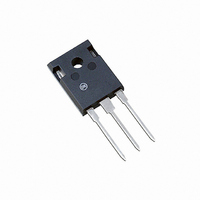
... MUR30x0WT = Device Code Assembly Location Y = Year WW = Work Week G = Pb−Free Package ORDERING INFORMATION Device Package MUR3020WT TO−247 MUR3020WTG TO−247 (Pb−Free) MUR3040WTG TO−247 (Pb−Free) MUR3060WT TO−247 MUR3060WTG TO−247 (Pb−Free MARKING DIAGRAM MUR30x0WT AYWWG Shipping 30 Units/Rail 30 Units/Rail 30 Units/Rail 30 Units/Rail 30 Units/Rail Publication Order Number: MUR3020WT/D ...
Page 2
... Amp 25° Maximum Instantaneous Reverse Current (Note 1) (Rated DC Voltage 150°C) J (Rated DC Voltage 25°C) J Maximum Reverse Recovery Time (i = 1.0 A, di/ Amps/ms Pulse Test: Pulse Width = 300 ms, Duty Cycle ≤ 2.0%. Symbol MUR3020WT V RRM V RWM F(AV FSM stg R qJC R qJA ...
Page 3
... SQUARE WAVE R = 40°C/W qJA 2 AS OBTAINED IN FREE AIR WITH NO HEAT SINK 100 120 140 T , AMBIENT TEMPERATURE (5C) A Figure 4. Current Derating, Ambient (Per Leg) MUR3020WT 100 100° 25° 0.5 0.2 0.1 0.05 0.02 0. *The curves shown are typical for the highest voltage device in the voltage grouping. ...
Page 4
T = 150° 0.5 0.3 0.2 0.1 0.2 0.4 0.6 0 INSTANTANEOUS VOLTAGE (VOLTS) F Figure 6. Typical Forward Voltage (Per Leg ...
Page 5
INSTANTANEOUS VOLTAGE (VOLTS) F Figure 11. Typical Forward Voltage (Per Leg 16°C/W AS OBTAINED qJA 9 ...
Page 6
D = 0.5 0.5 0.2 0.1 0.1 0.05 0.01 0.05 SINGLE PULSE 0.02 0.01 0.01 0.02 0.05 0.1 0.2 1K 500 200 100 (pk DUTY CYCLE 0.5 ...
Page 7
... L 5.40 6.20 0.212 0.244 N 4.32 5.49 0.170 0.216 P --- 4.50 --- 0.177 Q 3.55 3.65 0.140 0.144 U 6.15 BSC 0.242 BSC W 2.87 3.12 0.113 0.123 ON Semiconductor Website: www.onsemi.com Order Literature: http://www.onsemi.com/orderlit For additional information, please contact your local Sales Representative MUR3020WT/D ...