VB20150SG-E3/8W Vishay, VB20150SG-E3/8W Datasheet

DIODE 20A 150V SGL SCHOTTKY

VB20150SG-E3/8W

Manufacturer Part Number
VB20150SG-E3/8W
Description
DIODE 20A 150V SGL SCHOTTKY
Manufacturer
Vishay
Datasheet

Specifications of VB20150SG-E3/8W

Voltage - Forward (vf) (max) @ If
1.6V @ 20A
Voltage - Dc Reverse (vr) (max)
150V
Current - Average Rectified (io)
20A
Current - Reverse Leakage @ Vr
200µA @ 150V
Diode Type
Schottky
Speed
Fast Recovery =< 500ns, > 200mA (Io)
Mounting Type
Surface Mount
Package / Case
D²Pak, TO-263 (2 leads + tab)
Product
Schottky Rectifiers
Peak Reverse Voltage
150 V
Forward Continuous Current
20 A
Max Surge Current
140 A
Configuration
Single
Forward Voltage Drop
1.6 V
Maximum Reverse Leakage Current
200 uA
Operating Temperature Range
- 55 C to + 150 C
Mounting Style
SMD/SMT
Lead Free Status / RoHS Status
Lead free / RoHS Compliant
Reverse Recovery Time (trr)
-
Capacitance @ Vr, F
-
Lead Free Status / RoHS Status
Lead free / RoHS Compliant, Lead free / RoHS Compliant
Document Number: 89060
Revision: 24-Jun-09
PRIMARY CHARACTERISTICS
MAXIMUM RATINGS (T
PARAMETER
Maximum repetitive peak reverse voltage
Maximum average forward rectified current (fig. 1)
Peak forward surge current 8.3 ms single half
sine-wave superimposed on rated load
Non-repetitive avalanche energy
at T
Peak repetitive reverse current
at t
Voltage rate of change (rated V
Isolation voltage (ITO-220AB only)
from terminal to heatsink t = 1 min
Operating junction and storage temperature range
p
J
= 2 µs, 1 kHz, T
= 25 °C, L = 60 mH
PIN 3
NC
PIN 1
A
V
K
VB20150SG
F
V20150SG
TO-220AB
TO-263AB
at I
T
V
I
J
I
F(AV)
FSM
High-Voltage Trench MOS Barrier Schottky Rectifier
RRM
F
max.
= 20 A
NC
HEATSINK
K
CASE
PIN 2
J
= 38 °C ± 2 °C
A
1
2
TMBS
3
PDD-Americas@vishay.com, PDD-Asia@vishay.com,
For technical questions within your region, please contact one of the following:
R
)
V20150SG, VF20150SG, VB20150SG & VI20150SG
A
®
= 25 °C unless otherwise noted)
K
PIN 1
PIN 3
PIN 1
PIN 3
VF20150SG
Ultra Low V
ITO-220AB
VI20150SG
150 °C
TO-262AA
0.77 V
150 V
140 A
20 A
SYMBOL
T
J
V
I
dV/dt
PIN 2
I
I
F(AV)
E
V
, T
RRM
PIN 2
FSM
RRM
K
AC
1
AS
1
STG
New Product
2
2
3
3
F
= 0.57 V at I
V20150SG
FEATURES
TYPICAL APPLICATIONS
For use in high frequency converters, switching power
supplies, freewheeling diodes, OR-ing diode, dc-to-dc
converters and reverse battery protection.
MECHANICAL DATA
Case:
TO-262AA
Molding compound meets UL 94 V-0 flammability
rating
Base P/N-E3 - RoHS compliant, commercial grade
Terminals: Matte tin plated leads, solderable per
J-STD-002 and JESD 22-B102
E3 suffix meets JESD 201 class 1A whisker test
Polarity: As marked
Mounting Torque: 10 in-lbs maximum
• Trench MOS Schottky technology
• Low forward voltage drop, low power
• High efficiency operation
• Meets MSL level 1, per J-STD-020, LF
• Solder bath temperature 275 °C maximum, 10 s,
• Compliant to RoHS directive 2002/95/EC and in
losses
maximum peak of 245 °C (for TO-263AB package)
per JESD 22-B106 (for TO-220AB, ITO-220AB,
and TO-262AA package)
accordance to WEEE 2002/96/EC
VF20150SG
F
PDD-Europe@vishay.com
TO-220AB,
= 5 A
Vishay General Semiconductor
- 55 to + 150
10 000
1500
150
140
110
0.5
20
VB20150SG
ITO-220AB,
VI20150SG
TO-263AB
www.vishay.com
UNIT
V/µs
mJ
°C
V
A
A
A
V
and
1

Related parts for VB20150SG-E3/8W

VB20150SG-E3/8W Summary of contents

Page 1

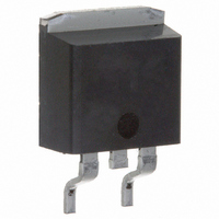
... V20150SG, VF20150SG, VB20150SG & VI20150SG High-Voltage Trench MOS Barrier Schottky Rectifier ® TMBS TO-220AB V20150SG PIN 1 PIN 1 PIN 2 CASE PIN 3 PIN 3 TO-263AB VB20150SG PIN HEATSINK PIN 3 PRIMARY CHARACTERISTICS I F(AV) V RRM I FSM max. J MAXIMUM RATINGS ( °C unless otherwise noted) A PARAMETER Maximum repetitive peak reverse voltage Maximum average forward rectified current (fig ...

Page 2

... Pulse test: Pulse width ≤ (2) THERMAL CHARACTERISTICS (T PARAMETER Typical thermal resistance ORDERING INFORMATION (Example) PACKAGE PREFERRED P/N TO-220AB V20150SG-E3/4W ITO-220AB VF20150SG-E3/4W TO-263AB VB20150SG-E3/4W TO-263AB VB20150SG-E3/8W TO-262AA VI20150SG-E3/4W RATINGS AND CHARACTERISTICS CURVES ( °C unless otherwise noted Resistive or Inductive Load V(B,I)20150SG 20 VF20150SG Mounted on Specific Heatsink ...

Page 3

... V20150SG, VF20150SG, VB20150SG & VI20150SG 100 T = 150 ° 125 ° 100 ° °C A 0.1 0 0.2 0.4 0.6 0.8 1.0 Instantaneous Forward Voltage (V) Figure 3. Typical Instantaneous Forward Characteristics 100 150 ° 125 ° 100 °C 0 °C 0.001 A 0.0001 Percent of Rated Peak Reverse Voltage (%) Figure 4 ...

Page 4

... V20150SG, VF20150SG, VB20150SG & VI20150SG Vishay General Semiconductor PACKAGE OUTLINE DIMENSIONS in inches (millimeters) TO-220AB 0.415 (10.54) MAX. 0.370 (9.40) 0.154 (3.91) 0.360 (9.14) 0.148 (3.74) 0.113 (2.87) 0.103 (2.62) 0.145 (3.68) 0.135 (3.43) 0.635 (16.13) 0.625 (15.87) PIN 0.350 (8.89 0.330 (8.38) ...

Page 5

... Vishay product could result in personal injury or death. Customers using or selling Vishay products not expressly indicated for use in such applications their own risk and agree to fully indemnify and hold Vishay and its distributors harmless from and against any and all claims, liabilities, expenses and damages arising or resulting in connection with such use or sale, including attorneys fees, even if such claim alleges that Vishay or its distributor was negligent regarding the design or manufacture of the part ...

Related keywords