MBR0540T1 ON Semiconductor, MBR0540T1 Datasheet - Page 2
MBR0540T1
Manufacturer Part Number
MBR0540T1
Description
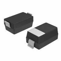
DIODE SCHOTTKY 40V 0.5A SOD123
Manufacturer
ON Semiconductor
Datasheet
1.MBR0540T1G.pdf
(6 pages)
Specifications of MBR0540T1
Voltage - Forward (vf) (max) @ If
510mV @ 500mA
Voltage - Dc Reverse (vr) (max)
40V
Current - Average Rectified (io)
500mA
Current - Reverse Leakage @ Vr
20µA @ 40V
Diode Type
Schottky
Speed
Fast Recovery =< 500ns, > 200mA (Io)
Mounting Type
Surface Mount
Package / Case
SOD-123
Lead Free Status / RoHS Status
Contains lead / RoHS non-compliant
Reverse Recovery Time (trr)
-
Capacitance @ Vr, F
-
Other names
MBR0540T1OSCT
Available stocks
Company
Part Number
Manufacturer
Quantity
Price
Company:

Part Number:
MBR0540T1
Manufacturer:
ON
Quantity:
5 321
Company:
Part Number:
MBR0540T1
Manufacturer:
ON
Quantity:
3 000
Part Number:
MBR0540T1
Manufacturer:
ON/安森美
Quantity:
20 000
Company:
Part Number:
MBR0540T1G
Manufacturer:
ON
Quantity:
360 000
Company:
Part Number:
MBR0540T1G
Manufacturer:
ONSEMI
Quantity:
51 000
Company:
Part Number:
MBR0540T1G
Manufacturer:
ON
Quantity:
30 000
Part Number:
MBR0540T1G
Manufacturer:
ON/安森美
Quantity:
20 000


Maximum ratings are those values beyond which device damage can occur. Maximum ratings applied to the device are individual stress limit
values (not normal operating conditions) and are not valid simultaneously. If these limits are exceeded, device functional operation is not implied,
damage may occur and reliability may be affected.
1. Mounted with minimum recommended pad size, PC Board FR4.
2. 1 inch square pad size (1 X 0.5 inch for each lead) on FR4 board.
3. Pulse Test: Pulse Width ≤ 250 ms, Duty Cycle ≤ 2.0%.
MAXIMUM RATINGS
THERMAL CHARACTERISTICS
ELECTRICAL CHARACTERISTICS
Peak Repetitive Reverse Voltage
Average Rectified Forward Current
Peak Repetitive Forward Current
Non−Repetitive Peak Surge Current
Storage/Operating Case Temperature Range
Operating Junction Temperature
Voltage Rate of Change
Thermal Resistance − Junction−to−Lead (Note 1)
Thermal Resistance − Junction−to−Ambient (Note 2)
Maximum Instantaneous Forward Voltage (Note 3)
Maximum Instantaneous Reverse Current (Note 3)
(i
(i
(V
(V
Working Peak Reverse Voltage
DC Blocking Voltage
(At Rated V
(At Rated V
(Surge Applied at Rated Load Conditions Halfwave,
Single Phase, 60 Hz)
(Rated V
F
F
R
R
= 0.5 A)
= 1 A)
= 40 V)
= 20 V)
R
, T
R
R
, T
, Square Wave, 20 kHz, T
J
= 25°C)
C
= 115°C)
Rating
Rating
C
= 115°C)
MBR0540T1, MBR0540T3
http://onsemi.com
2
Symbol
Symbol
T
V
V
stg
dv/dt
I
I
FRM
R
RWM
FSM
RRM
V
R
I
T
v
I
O
R
, T
tja
R
tjl
F
J
C
T
T
J
J
0.51
0.62
= 25°C
= 25°C
20
10
−55 to +150
−55 to +150
Value
Value
1000
206
118
0.5
1.0
5.5
40
T
T
J
J
13,000
5,000
= 100°C
= 100°C
0.46
0.61
°C/W
Unit
V/ms
Unit
mA
°C
°C
V
A
A
A
V
Related parts for MBR0540T1
Image
Part Number
Description
Manufacturer
Datasheet
Request
R

Part Number:
Description:
ON Semiconductor [VOLTAGE REGULATOR]
Manufacturer:
ON Semiconductor
Datasheet:
Part Number:
Description:
357-036-542-201 CARDEDGE 36POS DL .156 BLK LOPRO
Manufacturer:
ON Semiconductor
Datasheet:
Part Number:
Description:
357-036-542-201 CARDEDGE 36POS DL .156 BLK LOPRO
Manufacturer:
ON Semiconductor
Datasheet:
Part Number:
Description:
357-036-542-201 CARDEDGE 36POS DL .156 BLK LOPRO
Manufacturer:
ON Semiconductor
Datasheet:
Part Number:
Description:
357-036-542-201 CARDEDGE 36POS DL .156 BLK LOPRO
Manufacturer:
ON Semiconductor
Datasheet:
Part Number:
Description:
357-036-542-201 CARDEDGE 36POS DL .156 BLK LOPRO
Manufacturer:
ON Semiconductor
Datasheet:
Part Number:
Description:
357-036-542-201 CARDEDGE 36POS DL .156 BLK LOPRO
Manufacturer:
ON Semiconductor
Datasheet:
Part Number:
Description:
357-036-542-201 CARDEDGE 36POS DL .156 BLK LOPRO
Manufacturer:
ON Semiconductor
Datasheet:
Part Number:
Description:
357-036-542-201 CARDEDGE 36POS DL .156 BLK LOPRO
Manufacturer:
ON Semiconductor
Datasheet:
Part Number:
Description:
357-036-542-201 CARDEDGE 36POS DL .156 BLK LOPRO
Manufacturer:
ON Semiconductor
Datasheet:
Part Number:
Description:
357-036-542-201 CARDEDGE 36POS DL .156 BLK LOPRO
Manufacturer:
ON Semiconductor
Datasheet:
Part Number:
Description:
Manufacturer:
ON Semiconductor
Datasheet:
Part Number:
Description:
Manufacturer:
ON Semiconductor
Datasheet:
Part Number:
Description:
Manufacturer:
ON Semiconductor
Datasheet: