IRGS4056DPBF International Rectifier, IRGS4056DPBF Datasheet - Page 2
IRGS4056DPBF
Manufacturer Part Number
IRGS4056DPBF
Description
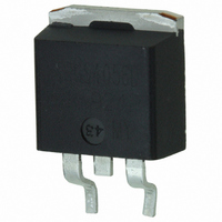
IGBT 600V 12A COPACK D2PAK
Manufacturer
International Rectifier
Datasheet
1.IRGS4056DPBF.pdf
(11 pages)
Specifications of IRGS4056DPBF
Igbt Type
Trench
Voltage - Collector Emitter Breakdown (max)
600V
Vce(on) (max) @ Vge, Ic
1.85V @ 15V, 12A
Current - Collector (ic) (max)
24A
Power - Max
140W
Input Type
Standard
Mounting Type
Surface Mount
Package / Case
D²Pak, TO-263 (2 leads + tab)
Transistor Type
IGBT
Dc Collector Current
24A
Collector Emitter Voltage Vces
600V
Power Dissipation Pd
140W
Collector Emitter Voltage V(br)ceo
600V
Operating Temperature Range
-55°C To +175°C
Rohs Compliant
Yes
Lead Free Status / RoHS Status
Lead free / RoHS Compliant
Available stocks
Company
Part Number
Manufacturer
Quantity
Price
Company:

Part Number:
IRGS4056DPBF
Manufacturer:
International Rectifier
Quantity:
135


IRGS4056DPbF
Notes:
‚
ƒ
„
Electrical Characteristics @ T
V
∆V
V
V
∆V
gfe
I
V
I
Switching Characteristics @ T
Q
Q
Q
E
E
E
t
t
t
t
E
E
E
t
t
t
t
C
C
C
RBSOA
SCSOA
Erec
t
I
CES
GES
d(on)
r
d(off)
f
d(on)
r
d(off)
f
rr
rr
(BR)CES
CE(on)
GE(th)
FM
on
off
total
on
off
total
ies
oes
res
g
ge
gc
V
This is only applied to TO-220AB package.
Pulse width limited by max. junction temperature.
Refer to AN-1086 for guidelines for measuring V
(BR)CES
GE(th)
2
CC
= 80% (V
/∆TJ
/∆T
J
CES
Collector-to-Emitter Breakdown Voltage
Temperature Coeff. of Breakdown Voltage
Collector-to-Emitter Saturation Voltage
Gate Threshold Voltage
Threshold Voltage temp. coefficient
Forward Transconductance
Collector-to-Emitter Leakage Current
Diode Forward Voltage Drop
Gate-to-Emitter Leakage Current
Total Gate Charge (turn-on)
Gate-to-Emitter Charge (turn-on)
Gate-to-Collector Charge (turn-on)
Turn-On Switching Loss
Turn-Off Switching Loss
Total Switching Loss
Turn-On delay time
Rise time
Turn-Off delay time
Fall time
Turn-On Switching Loss
Turn-Off Switching Loss
Total Switching Loss
Turn-On delay time
Rise time
Turn-Off delay time
Fall time
Input Capacitance
Output Capacitance
Reverse Transfer Capacitance
Reverse Bias Safe Operating Area
Short Circuit Safe Operating Area
Reverse Recovery Energy of the Diode
Diode Reverse Recovery Time
Peak Reverse Recovery Current
), V
GE
= 20V, L = 100µH, R
Parameter
Parameter
J
J
G
= 25°C (unless otherwise specified)
= 25°C (unless otherwise specified)
= 22Ω.
(BR)CES
safely.
Min.
Min.
600
4.0
—
—
—
—
—
—
—
—
—
—
—
—
—
—
—
—
—
—
—
—
—
—
—
—
—
—
—
—
—
—
—
—
—
—
FULL SQUARE
5
Typ.
Typ.
0.30
1.55
1.90
1.97
2.10
1.61
475
225
300
185
355
540
102
765
280
-18
7.7
2.0
7.0
31
30
23
19
—
—
—
25
11
75
17
83
24
18
41
52
—
68
Max. Units
Max. Units
1.85
3.10
±100
118
273
391
6.5
25
16
40
—
—
—
—
—
—
—
—
38
11
24
94
31
—
—
—
—
—
—
—
—
—
—
—
—
—
—
mV/°C V
V/°C V
µA
nA
nC
pF
µJ
ns
µJ
ns
µs
µJ
ns
V
V
V
S
V
A
V
I
I
I
V
V
V
V
I
I
V
I
V
V
I
R
Energy losses include tail & diode reverse recovery
I
R
I
R
Energy losses include tail & diode reverse recovery
I
R
T
V
V
f = 1.0Mhz
T
V
Rg = 22Ω, V
V
Rg = 22Ω, V
T
V
V
C
C
C
F
F
C
C
C
C
C
J
J
J
GE
GE
CE
CE
CE
GE
GE
GE
GE
CC
G
G
G
G
GE
CC
CC
CC
CC
GE
= 12A
= 12A, T
= 12A, V
= 12A, V
= 12A, V
= 12A
= 12A, V
= 12A, V
= 12A, V
= 12A, V
=22Ω, L=100µH, L
= 175°C
= 175°C, I
= 175°C
= 22Ω, L = 200µH, L
= 22Ω, L = 200µH, L
= 22Ω, L = 200µH, L
= V
= V
= 50V, I
= 400V
= 30V
= 480V, Vp =600V
= 400V, Vp =600V
= 400V, I
= 0V, I
= 0V, I
= 0V, V
= 0V, V
= ±20V
= 15V
= 0V
= 15V, Rg = 22Ω, L =200µH, L
Conditions
GE
GE
, I
, I
J
C
C
GE
GE
GE
CC
CC
CC
CC
C
C
CE
CE
C
= 175°C
GE
GE
= 100µA
= 1mA (25°C-175°C)
C
= 350µA
= 1.0mA (25°C - 175°C)
F
= 12A, PW = 80µs
= 15V, T
= 15V, T
= 15V, T
= 400V, V
= 400V, V
= 400V, V
= 400V, V
= 600V
= 600V, T
= 48A
= 12A
= +15V to 0V
= +15V to 0V
Conditions
S
=150nH, T
J
J
J
= 25°C
= 150°C
= 175°C
GE
S
GE
S
GE
GE
S
J
= 150nH, T
= 150nH, T
= 150nH
= 175°C
=15V
= 15V
= 15V
= 15V
J
= 175°C
s
= 150nH
J
J
= 25°C
= 25°C
www.irf.com
Ã
WF1, WF2
17, 18, 19
22, CT3
Ref.Fig
9,10,11
Ref.Fig
11, 12
13, 15
14, 16
20, 21
9, 10,
5,6,7
WF1
WF2
WF4
CT6
CT6
CT1
CT4
CT4
CT4
CT4
CT2
WF3
24
23
8
4
Related parts for IRGS4056DPBF
Image
Part Number
Description
Manufacturer
Datasheet
Request
R

Part Number:
Description:
SCHOTTKY RECTIFIER
Manufacturer:
International Rectifier Corp.
Datasheet:
Part Number:
Description:
SCHOTTKY RECTIFIER
Manufacturer:
International Rectifier Corp.
Datasheet:
Part Number:
Description:
SCHOTTKY RECTIFIER
Manufacturer:
International Rectifier Corp.
Datasheet:
Part Number:
Description:
SCHOTTKY RECTIFIER
Manufacturer:
International Rectifier Corp.
Datasheet:
Part Number:
Description:
SCHOTTKY RECTIFIER
Manufacturer:
International Rectifier Corp.
Datasheet:
Part Number:
Description:
SCHOTTKY RECTIFIER
Manufacturer:
International Rectifier Corp.
Datasheet:
Part Number:
Description:
SCHOTTKY RECTIFIER
Manufacturer:
International Rectifier Corp.
Datasheet:
Part Number:
Description:
SCHOTTKY RECTIFIER
Manufacturer:
International Rectifier Corp.
Datasheet:
Part Number:
Description:
SCHOTTKY RECTIFIER
Manufacturer:
International Rectifier Corp.
Datasheet:
Part Number:
Description:
SCHOTTKY RECTIFIER
Manufacturer:
International Rectifier Corp.
Datasheet:
Part Number:
Description:
SCHOTTKY RECTIFIER
Manufacturer:
International Rectifier Corp.
Datasheet:
Part Number:
Description:
SCHOTTKY RECTIFIER
Manufacturer:
International Rectifier Corp.
Datasheet:
Part Number:
Description:
SCHOTTKY RECTIFIER
Manufacturer:
International Rectifier Corp.
Datasheet:
Part Number:
Description:
SCHOTTKY RECTIFIER
Manufacturer:
International Rectifier Corp.
Datasheet:
Part Number:
Description:
SCHOTTKY RECTIFIER
Manufacturer:
International Rectifier Corp.
Datasheet: