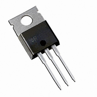
IRG4BC20SD International Rectifier, IRG4BC20SD Datasheet

IRG4BC20SD
Specifications of IRG4BC20SD
Available stocks
Related parts for IRG4BC20SD
IRG4BC20SD Summary of contents
Page 1
... JA Wt Weight www.irf.com G TM ultrafast, n-cha nn el 300 (0.063 in. (1.6mm) from case) Min. ––– ––– ––– ––– ––– PD- 91793 IRG4BC20SD Standard Speed IGBT 600V CES V = 1.4V CE(on) typ 15V 10A TO-220AB Max ...
Page 2
... IRG4BC20SD Electrical Characteristics @ T Parameter V Collector-to-Emitter Breakdown Voltageƒ (BR)CES Temperature Coeff. of Breakdown Voltage (BR)CES J V Collector-to-Emitter Saturation Voltage CE(on) V Gate Threshold Voltage GE(th Temperature Coeff. of Threshold Voltage GE(th Forward Transconductance fe I Zero Gate Voltage Collector Current CES V Diode Forward Voltage Drop ...
Page 3
... Collector-to-Emitter Voltage (V) CE Fig Typical Output Characteristics www.irf.com 1 f, Frequency (KHz) (Load Current = I of fundamental) RMS 100 T = 150 15V 1 5 3.0 4.0 Fig Typical Transfer Characteristics IRG4BC20SD For both: D uty cy cle: 50 125° 90°C s ink G ate drive as specified Dis sip ation = 50V CC 5µ ...
Page 4
... IRG4BC20SD 100 T , Case Temperature ( C Fig Maximum Collector Current vs. Case Temperature 10 0.50 1 0.20 0.10 0.05 0.1 0.02 0.01 SINGLE PULSE (THERMAL RESPONSE) 0.01 0.00001 0.0001 Fig Maximum Effective Transient Thermal Impedance, Junction-to-Case 4 3 15V PULSE WIDTH 2.0 1.0 125 150 -60 -40 -20 ° ...
Page 5
... Gate Resistance ( ) G Fig Typical Switching Losses vs. Gate Resistance www.irf.com SHORTED 100 0 Fig Typical Gate Charge vs. 100 15V 480V 0 -60 -40 -20 Fig Typical Switching Losses vs. IRG4BC20SD = 400V = 10A Total Gate Charge (nC) G Gate-to-Emitter Voltage 100 120 140 160 ° Junction Temperature ( Junction Temperature 30 5 ...
Page 6
... IRG4BC20SD 150 C ° 480V 15V Collector Current (A) C Fig Typical Switching Losses vs. Collector-to-Emitter Current 0.1 Fig Maximum Forward Voltage Drop vs. Instantaneous Forward Current 6 100 ° ° ° 0.4 0.8 1.2 1.6 2.0 2.4 2 lta 20V o = 125 C SAFE OPERATING AREA 10 100 V , Collector-to-Emitter Voltage (V) CE Fig ...
Page 7
... ° ° /µ Fig Typical Reverse Recovery vs ° ° . / /µs) f Fig Typical Stored Charge vs. di www.irf.com . Fig Typical Recovery Current vs /dt Fig Typical di f IRG4BC20SD ° ° 4 / /µ ° ° 4 /µ /dt vs. di /dt (rec / ...
Page 8
... IRG4BC20SD 430µF 80% of Vce Fig. 18a - Test Circuit for Measurement off(diode d(on Fig. 18c - Test Waveforms for Circuit of Fig. 18a, Defining d(on) 8 Same ty pe device as D .U. . 90% 10 d(off) f d(on) Fig. 18b - Test Waveforms for Circuit of Fig. 18a, Defining Vce Ic dt ...
Page 9
... Figure 18e. Macro Waveforms for µ Figure 19. Clamped Inductive Load Test Circuit www.irf.com Figure 18a's D.U. 480V Figure 20. Pulsed Collector Current IRG4BC20SD Test Circuit 480V @25°C C Test Circuit 9 ...
Page 10
... IRG4BC20SD Repetitive rating: V =20V; pulse width limited by maximum junction temperature (figure 20 =80%( =20V, L=10µ CES GE Pulse width 80µs; duty factor 0.1%. Pulse width 5.0µs, single shot (. (. (. (. 6.47 (.255 ) 6.10 (.240 ) (. (. 1.15 (.045 (. 4.06 (.160 ) (. 3.55 (.140 ) 0.93 (.037 0.69 (.027) 1 ...
Page 11
Note: For the most current drawings please refer to the IR website at: http://www.irf.com/package/ ...


