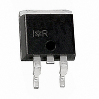
IRG4BC20FD-STRL International Rectifier, IRG4BC20FD-STRL Datasheet - Page 2

IRG4BC20FD-STRL
Manufacturer Part Number
IRG4BC20FD-STRL
Description
IGBT FAST 600V 16A LEFT D2PAK
Manufacturer
International Rectifier
Datasheet
1.IRG4BC20FD-S.pdf
(11 pages)
Specifications of IRG4BC20FD-STRL
Voltage - Collector Emitter Breakdown (max)
600V
Vce(on) (max) @ Vge, Ic
2V @ 15V, 9A
Current - Collector (ic) (max)
16A
Power - Max
60W
Input Type
Standard
Mounting Type
Surface Mount
Package / Case
D²Pak, TO-263 (2 leads + tab)
Channel Type
N
Configuration
Single
Collector-emitter Voltage
600V
Collector Current (dc) (max)
16A
Gate To Emitter Voltage (max)
±20V
Pin Count
2 +Tab
Mounting
Surface Mount
Operating Temperature (max)
150C
Operating Temperature Classification
Military
Lead Free Status / RoHS Status
Contains lead / RoHS non-compliant
Igbt Type
-
Lead Free Status / Rohs Status
Not Compliant
Available stocks
Company
Part Number
Manufacturer
Quantity
Price
Company:
Part Number:
IRG4BC20FD-STRL
Manufacturer:
IR
Quantity:
12 500
Company:
Part Number:
IRG4BC20FD-STRLPBF
Manufacturer:
IR
Quantity:
15 000
IRG4BC20FD-S
Switching Characteristics @ T
Electrical Characteristics @ T
V
V
V
g
I
V
I
Q
Qge
Q
t
t
t
t
E
E
E
t
t
t
t
E
L
C
C
C
t
I
Q
di
CES
GES
d(on)
d(off)
f
d(on)
d(off)
f
r
r
rr
rr
V
V
fe
E
(BR)CES
CE(on)
GE(th)
on
off
ts
ts
FM
ies
oes
res
g
gc
(rec)M
rr
(BR)CES
2
GE(th)
/dt
/ T
/ T
J
J
Collector-to-Emitter Breakdown VoltageS
Temperature Coeff. of Breakdown Voltage
Collector-to-Emitter Saturation Voltage
Gate Threshold Voltage
Temperature Coeff. of Threshold Voltage
Forward Transconductance T
Zero Gate Voltage Collector Current
Diode Forward Voltage Drop
Gate-to-Emitter Leakage Current
Total Gate Charge (turn-on)
Gate - Emitter Charge (turn-on)
Gate - Collector Charge (turn-on)
Turn-On Delay Time
Rise Time
Turn-Off Delay Time
Fall Time
Turn-On Switching Loss
Turn-Off Switching Loss
Total Switching Loss
Turn-On Delay Time
Rise Time
Turn-Off Delay Time
Fall Time
Total Switching Loss
Internal Emitter Inductance
Input Capacitance
Output Capacitance
Reverse Transfer Capacitance
Diode Reverse Recovery Time
Diode Peak Reverse Recovery Current —
Diode Reverse Recovery Charge
Diode Peak Rate of Fall of Recovery
During t
Parameter
Parameter
b
J
J
= 25°C (unless otherwise specified)
= 25°C (unless otherwise specified)
Min. Typ. Max. Units
Min. Typ. Max. Units
600
3.0
2.9
—
—
—
—
—
—
—
—
—
—
—
—
—
—
—
—
—
—
—
—
—
—
—
—
—
—
—
—
—
—
—
—
—
—
—
—
0.72
1.66
2.06
1.76
0.25
0.64
0.89
1.35
240
150
320
290
540
124
240
210
-11
5.1
1.4
1.3
4.2
9.9
7.5
7.0
3.5
4.5
27
43
20
41
22
37
37
55
65
—
—
—
—
—
1700
±100
250
360
220
138
360
2.0
6.0
1.7
1.6
6.2
1.3
5.0
8.0
40
15
55
90
—
—
—
—
—
—
—
—
—
—
—
—
—
—
—
—
—
—
—
—
—
mV/°C V
V/°C
A/µs
µA
nA
mJ
mJ
nC
nH
pF
nC
ns
ns
ns
V
V
S
V
A
V
V
I
I
I
V
V
V
V
I
I
V
I
V
V
T
I
V
Energy losses include "tail" and
diode reverse recovery.
See Fig. 9, 10, 18
T
I
V
Energy losses include "tail" and
diode reverse recovery.
Measured 5mm from package
V
V
ƒ = 1.0MHz
T
T
T
T
T
T
T
T
C
C
C
C
C
C
C
C
J
J
J
J
J
J
J
J
J
J
GE
GE
CE
CE
CE
GE
GE
GE
CC
GE
GE
GE
GE
CC
= 9.0A
= 16A
= 9.0A, T
= 8.0A
= 8.0A, T
= 9.0A
= 9.0A, V
= 9.0A, V
= 125°C
= 125°C
= 125°C
= 125°C
= 25°C
= 150°C,
= 25°C
= 25°C
= 25°C
= 25°C
= V
= V
= 100V, I
= ±20V
= 15V
= 0V
= 0V, I
= 0V, I
= 0V, V
= 0V, V
= 400V
= 15V, R
= 15V, R
= 30V
GE
GE
, I
, I
C
C
J
J
CE
CC
CC
C
C
CE
See Fig.
See Fig.
= 250µA
= 1.0mA
See Fig.
See Fig.
Conditions
= 150°C
= 150°C
Conditions
G
G
C
= 250µA
= 250µA
= 600V
= 600V, T
= 480V
= 480V
See Fig. 10, 11, 18
= 50
= 50
= 9.0A
14
15
17
16
See Fig. 8
See Fig. 7
www.irf.com
di/dt = 200A/µs
V
See Fig. 2, 5
See Fig. 13
V
J
GE
I
R
= 150°C
F
= 200V
= 8.0A
= 15V


