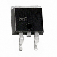
IRG4BC20W-S International Rectifier, IRG4BC20W-S Datasheet

IRG4BC20W-S
Specifications of IRG4BC20W-S
Available stocks
Related parts for IRG4BC20W-S
IRG4BC20W-S Summary of contents
Page 1
... STG Soldering Temperature, for 10 seconds Thermal Resistance Parameter R Junction-to-Case JC R Case-to-Sink, Flat, Greased Surface CS R Junction-to-Ambient, typical socket mount JA Wt Weight www.irf.com IRG4BC20W N-channel - 150 300 (0.063 in. (1.6mm) from case ) Typ. ––– 0.5 ––– 1. 94076 V = 600V ...
Page 2
... IRG4BC20W-S Electrical Characteristics @ T Parameter V Collector-to-Emitter Breakdown Voltage (BR)CES Emitter-to-Collector Breakdown Voltage „ V (BR)ECS Temperature Coeff. of Breakdown Voltage (BR)CES J V Collector-to-Emitter Saturation Voltage CE(ON) V Gate Threshold Voltage GE(th Temperature Coeff. of Threshold Voltage GE(th) J Forward Transconductance … Zero Gate Voltage Collector Current CES ...
Page 3
... Fig Typical Output Characteristics www.irf.com uty c yc le: 50 125° 90°C s ink G ate drive as spec ified tio Frequency (kHz) (Load Current = I of fundamental) RMS 100 T = 150 15V Fig Typical Transfer Characteristics IRG4BC20W-S T ria ° ° 50V CC 5µs PULSE WIDTH Gate-to-Emitter Voltage ( ...
Page 4
... IRG4BC20W 100 T , Case Temperature ( C) C Fig Maximum Collector Current vs. Case Temperature 0.50 1 0.20 0.10 0.05 0.1 0.02 0.01 SINGLE PULSE (THERMAL RESPONSE) 0.01 0.00001 0.0001 Fig Maximum Effective Transient Thermal Impedance, Junction-to-Case 4 3 15V PULSE WIDTH 2.0 1.0 -60 -40 -20 125 150 ° ...
Page 5
... Gate Resistance G Fig Typical Switching Losses vs. Gate Resistance www.irf.com SHORTED 100 0 Fig Typical Gate Charge vs 0.1 0.01 -60 -40 - Fig Typical Switching Losses vs. IRG4BC20W-S = 400V = 6. Total Gate Charge (nC) G Gate-to-Emitter Voltage 50 = Ohm = 15V = 480V 6 3. 100 120 140 160 ° Junction Temperature ( ...
Page 6
... IRG4BC20W-S 0 Ohm 150 C ° 480V 15V GE 0.6 0.4 0.2 0 Collector-to-emitter Current (A) C Fig Typical Switching Losses vs. Collector-to-Emitter Current 6 100 SAFE OPERATING AREA 20V o = 125 C 10 100 , Collector-to-Emitter Voltage (V) Fig Turn-Off SOA www.irf.com 1000 ...
Page 7
... www.irf.com 480V ‚ .T. D river ‚ ƒ ff t=5µ IRG4BC20W-S 480V 25° 480µF 960V Fig. 13b - Pulsed Collector Current Test Circuit Fig. 14a - Switching Loss Test Circuit * Driver same type as D.U.T 480V Fig. 14b - Switching Loss Waveforms 7 ...
Page 8
... IRG4BC20W Pak Package Outline 1 0.54 (.415 ) 1 0.29 (.405 ) 1.4 0 (.055 ) - AX. 2 1 5.49 (.6 10) 1 4.73 (.5 80 1.40 (.0 55) 3X 1.14 (.0 45) 0 0 .08 (.20 0) 0.25 (. FTER & 4. TRO L LIN ATSINK & SIO Pak Part Marking Information TIO (. (.16 5) 1 ...
Page 9
... Data and specifications subject to change without notice. This product has been designed and qualified for the Industrial market. Qualification Standards can be found on IR’s Web site. Visit us at www.irf.com for sales contact information.1/01 IRG4BC20W (. (. (. (. (. (. (. (. ...
Page 10
Note: For the most current drawings please refer to the IR website at: http://www.irf.com/package/ ...


