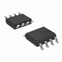
DMP2066LSD-13 Diodes Inc, DMP2066LSD-13 Datasheet - Page 2

DMP2066LSD-13
Manufacturer Part Number
DMP2066LSD-13
Description
MOSFET P-CH DUAL 20V 5.8A 8-SOIC
Manufacturer
Diodes Inc
Datasheet
1.DMP2066LSD-13.pdf
(4 pages)
Specifications of DMP2066LSD-13
Fet Type
2 P-Channel (Dual)
Fet Feature
Logic Level Gate
Rds On (max) @ Id, Vgs
40 mOhm @ 4.6A, 4.5V
Drain To Source Voltage (vdss)
20V
Current - Continuous Drain (id) @ 25° C
5.8A
Vgs(th) (max) @ Id
1.2V @ 250µA
Gate Charge (qg) @ Vgs
10.1nC @ 4.5V
Input Capacitance (ciss) @ Vds
820pF @ 15V
Power - Max
2W
Mounting Type
Surface Mount
Package / Case
8-SOP
Lead Free Status / RoHS Status
Lead free / RoHS Compliant
Other names
DMP2066LSDDITR
Available stocks
Company
Part Number
Manufacturer
Quantity
Price
Company:
Part Number:
DMP2066LSD-13
Manufacturer:
DIODES
Quantity:
2 500
Part Number:
DMP2066LSD-13
Manufacturer:
DIODES/美台
Quantity:
20 000
Part Number:
DMP2066LSD-13-F
Manufacturer:
DIODES/美台
Quantity:
20 000
Electrical Characteristics
OFF CHARACTERISTICS (Note 5)
Drain-Source Breakdown Voltage
Zero Gate Voltage Drain Current
Gate-Source Leakage
ON CHARACTERISTICS (Note 5)
Gate Threshold Voltage
Static Drain-Source On-Resistance
Forward Transconductance
Diode Forward Voltage (Note 5)
DYNAMIC CHARACTERISTICS
Input Capacitance
Output Capacitance
Reverse Transfer Capacitance
Gate Resistance
SWITCHING CHARACTERISTICS
Total Gate Charge
Gate-Source Charge
Gate-Drain Charge
Turn-On Delay Time
Rise Time
Turn-Off Delay Time
Fall Time
Notes:
DMP2066LSD
Document number: DS31453 Rev. 3 - 2
5. Short duration pulse test used to minimize self-heating effect.
30
24
18
12
6
0
0
0.5
Characteristic
V , DRAIN-SOURCE VOLTAGE (V)
DS
Fig. 1 Typical Output Characteristic
1
V
GS
1.5
= 10V
2
2.5
@T
V
3
GS
A
= 4.5V
= 25°C unless otherwise specified
V
3.5
GS
= 1.5V
V
V
V
GS
4
GS
GS
Symbol
R
BV
V
= 3.0V
= 2.5V
DS (ON)
= 2.0V
C
Q
t
t
I
I
Q
V
C
C
GS(th)
d(on)
d(off)
DSS
GSS
R
Q
g
4.5
t
SD
oss
GD
t
DSS
iss
rss
GS
fs
r
f
G
G
5
www.diodes.com
Min
-0.6
-0.5
-20
⎯
⎯
⎯
⎯
⎯
⎯
⎯
⎯
⎯
⎯
⎯
⎯
⎯
⎯
⎯
⎯
2 of 4
-0.94
-0.72
10.1
28.0
23.4
Typ
820
200
160
2.5
1.5
4.3
4.4
9.9
⎯
⎯
⎯
29
55
9
20
16
12
8
4
0
0
V
0.5
DS
T = 125°C
Fig. 2 Typical Transfer Characteristic
±100
V
Max
-1.2
-1.4
A
= 5.0V
40
70
⎯
⎯
⎯
⎯
⎯
⎯
⎯
⎯
⎯
⎯
⎯
⎯
⎯
-1
GS
T = 150°C
, GATE-SOURCE VOLTAGE (V)
1
A
1.5
Unit
mΩ
μA
nA
nC
pF
pF
pF
ns
Ω
V
V
S
V
T = -55°C
A
2
T = 25°C
A
T = 85°C
V
V
V
V
V
V
V
V
V
f = 1.0MHz
V
f = 1.0MHz
V
I
V
I
A
D
D
2.5
GS
DS
GS
DS
GS
GS
DS
GS
DS
DS
DS
DS
= -5.9A
= -1A, R
= 0V, I
= -20V, V
= V
= -10V, I
= ±12V, V
= -4.5V, I
= -2.5V, I
= 0V, I
= -15V, V
= 0V, V
= -10V, V
= -10V, V
DMP2066LSD
Test Condition
GS
3
, I
G
D
S
GS
D
= -250μA
= 6.0Ω
D
= -2.1A
© Diodes Incorporated
3.5
GS
D
D
= -250μA
GS
GS
GS
DS
= -4.6A
= 0V
= -4.6A
= -3.8A
= 0V
= 0V
= -4.5V,
= -4.5V,
= 0V
August 2008
4


