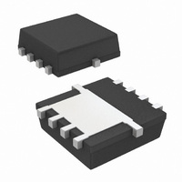
SI7222DN-T1-E3 Vishay, SI7222DN-T1-E3 Datasheet

SI7222DN-T1-E3
Specifications of SI7222DN-T1-E3
Related parts for SI7222DN-T1-E3
SI7222DN-T1-E3 Summary of contents
Page 1
... Bottom View Ordering Information: Si7222DN-T1-E3 (Lead (Pb)-free) Si7222DN-T1-GE3 (Lead (Pb)-free and Halogen-free) ABSOLUTE MAXIMUM RATINGS T Parameter Drain-Source Voltage Gate-Source Voltage Continuous Drain Current (T = 150 °C) J Pulsed Drain Current Continuous Source-Drain Diode Current Avalanche Current Single-Pulse Avalanche Energy Maximum Power Dissipation Operating Junction and Storage Temperature Range ...
Page 2
... Si7222DN Vishay Siliconix THERMAL RESISTANCE RATINGS Parameter a, b Maximum Junction-to-Ambient Maximum Junction-to-Case (Drain) Notes: a. Surface Mounted on 1" x 1" FR4 board. b. Maximum under Steady State conditions is 94 °C/W. SPECIFICATIONS °C, unless otherwise noted J Parameter Static Drain-Source Breakdown Voltage V Temperature Coefficient DS V Temperature Coefficient ...
Page 3
... Exposure to absolute maximum rating conditions for extended periods may affect device reliability. Document Number: 73439 S-83052-Rev. B, 29-Dec-08 Symbol Test Conditions ° 1.7 A, dI/dt = 100 A/µ Si7222DN Vishay Siliconix Min. Typ. Max 0.76 1 ° www.vishay.com Unit ...
Page 4
... Si7222DN Vishay Siliconix TYPICAL CHARACTERISTICS 25 °C, unless otherwise noted thru Drain-to-Source Voltage (V) DS Output Characteristics 0.050 0.047 0.044 0.041 0.038 0.035 0.032 0.029 0.026 0.023 0.020 Drain Current (A) D On-Resistance vs. Drain Current and Gate Voltage 5 0.0 2.2 4 Total Gate Charge (nC) ...
Page 5
... D 75 100 125 150 100 Limited DS(on 0 °C A Single Pulse 0.01 0.01 0 Drain-to-Source Voltage ( > minimum V at which DS(on) Safe Operating Area, Junction-to-Ambient Si7222DN Vishay Siliconix 0. 5 0.16 0. 125 °C 0. ° Gate-to-Source Voltage (V) GS On-Resistance vs. Gate-to-Source Voltage 0.001 ...
Page 6
... Si7222DN Vishay Siliconix TYPICAL CHARACTERISTICS 25 °C, unless otherwise noted Case Temperature (°C) C Power, Junction-to-Case * The power dissipation P is based dissipation limit for cases where additional heatsinking is used used to determine the current rating, when this rating falls below the package limit. www.vishay.com ...
Page 7
... Technology and Package Reliability represent a composite of all qualified locations. For related documents such as package/tape drawings, part marking, and reliability data, see www.vishay.com/ppg?73439. Document Number: 73439 S-83052-Rev. B, 29-Dec- Square Wave Pulse Duration (s) Normalized Thermal Transient Impedance, Junction-to-Ambient - Square Wave Pulse Duration (s) Normalized Thermal Transient Impedance, Junction-to-Case Si7222DN Vishay Siliconix Notes Duty Cycle Per Unit Base = °C/W ...
Page 8
... Vishay product could result in personal injury or death. Customers using or selling Vishay products not expressly indicated for use in such applications their own risk and agree to fully indemnify and hold Vishay and its distributors harmless from and against any and all claims, liabilities, expenses and damages arising or resulting in connection with such use or sale, including attorneys fees, even if such claim alleges that Vishay or its distributor was negligent regarding the design or manufacture of the part ...


