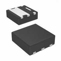
SIA511DJ-T1-GE3 Vishay, SIA511DJ-T1-GE3 Datasheet

SIA511DJ-T1-GE3
Specifications of SIA511DJ-T1-GE3
Related parts for SIA511DJ-T1-GE3
SIA511DJ-T1-GE3 Summary of contents
Page 1
... 2. Ordering Information: SiA511DJ-T1-GE3 (Lead (Pb)-free and Halogen-free) ABSOLUTE MAXIMUM RATINGS T Parameter Drain-Source Voltage Gate-Source Voltage Continuous Drain Current (T = 150 °C) J Pulsed Drain Current Source Drain Current Diode Current Maximum Power Dissipation Operating Junction and Storage Temperature Range Soldering Recommendations (Peak Temperature) ...
Page 2
... SiA511DJ Vishay Siliconix SPECIFICATIONS °C, unless otherwise noted J Parameter Static Drain-Source Breakdown Voltage V Temperature Coefficient DS V Temperature Coefficient GS(th) Gate Threshold Voltage Gate-Body Leakage Zero Gate Voltage Drain Current b On-State Drain Current b Drain-Source On-State Resistance b Forward Transconductance a Dynamic Input Capacitance Output Capacitance ...
Page 3
... GEN g P-Channel t d(off) = 1.8 Ω ≅ GEN ° 4 3 N-Channel 4.4 A, di/dt = 100 A/µ P-Channel 3.4 A, di/ 100 A/µ SiA511DJ Vishay Siliconix Min. Typ. Max Ω Ω Ω N-Ch 4.5 P-Ch - 4.5 N-Ch ...
Page 4
... SiA511DJ Vishay Siliconix N-CHANNEL TYPICAL CHARACTERISTICS 25 °C, unless otherwise noted 0.0 0.4 0.8 - Drain-to-Source Voltage ( Output Characteristics 0. 0.08 0.07 0. 0.05 V 0. Drain Current (A) D On-Resistance vs. Drain Current and Gate Voltage 5 Total Gate Charge (nC) g Gate Charge www.vishay.com 4 New Product thru 2 ...
Page 5
... Limited DS(on 0 °C A BVDSS Limited Single Pulse 0.01 0 Drain-to-Source Voltage ( minimum V at which DS(on) Safe Operating Area, Junction-to-Ambient SiA511DJ Vishay Siliconix I = 4.2 A, 125 ° 4 ° Gate-to-Source Voltage (V) GS On-Resistance vs. Gate-to-Source Voltage 5 0 0.001 0.01 0 Pulse (s) Single Pulse Power (Junction-to-Ambient) 100 µs ...
Page 6
... SiA511DJ Vishay Siliconix N-CHANNEL TYPICAL CHARACTERISTICS 25 °C, unless otherwise noted Package Limited Case Temperature (°C) C Current Derating* * The power dissipation P is based J(max) dissipation limit for cases where additional heatsinking is used used to determine the current rating, when this rating falls below the package limit ...
Page 7
... Single Pulse 0. Document Number: 74592 S-80436-Rev. B, 03-Mar-08 New Product - Square Wave Pulse Duration (s) Normalized Thermal Transient Impedance, Junction-to-Ambient -3 10 Square Wave Pulse Duration (s) Normalized Thermal Transient Impedance, Junction-to-Foot SiA511DJ Vishay Siliconix Notes Duty Cycle Per Unit Base = °C ( ...
Page 8
... SiA511DJ Vishay Siliconix P-CHANNEL TYPICAL CHARACTERISTICS 25 °C, unless otherwise noted 0.0 0.4 0 Drain-to-Source Voltage (V) DS Output Characteristics 0. 0.20 0. 0.10 0. Drain Current (A) D On-Resistance vs. Drain Current and Gate Voltage 4 Total Gate Charge (nC) g Gate Charge www.vishay.com 8 New Product thru 2 ...
Page 9
... Limited DS(on) 1 0.1 BVDSS Limited °C A Single Pulse 0.01 0 Drain-to-Source Voltage ( minimum V at which DS(on) Safe Operating Area, Junction-to-Ambient SiA511DJ Vishay Siliconix Gate-to-Source Voltage (V) GS On-Resistance vs. Gate-to-Source Voltage 5 0 0.01 0 Pulse (s) Single Pulse Power, Junction-to-Ambient 100 µ 100 ...
Page 10
... SiA511DJ Vishay Siliconix P-CHANNEL TYPICAL CHARACTERISTICS 25 °C, unless otherwise noted Package Limited Case Temperature (°C) C Current Derating* * The power dissipation P is based J(max) dissipation limit for cases where additional heatsinking is used used to determine the current rating, when this rating falls below the package limit ...
Page 11
... Document Number: 74592 S-80436-Rev. B, 03-Mar-08 New Product - Square Wave Pulse Duration (s) Normalized Thermal Transient Impedance, Junction-to-Ambient -3 10 Square Wave Pulse Duration (s) Normalized Thermal Transient Impedance, Junction-to-Case SiA511DJ Vishay Siliconix Notes Duty Cycle Per Unit Base = °C/W ...
Page 12
... Vishay disclaims any and all liability arising out of the use or application of any product described herein or of any information provided herein to the maximum extent permitted by law. The product specifications do not expand or otherwise modify Vishay’ ...


