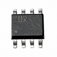
IRF7907PBF International Rectifier, IRF7907PBF Datasheet - Page 5

IRF7907PBF
Manufacturer Part Number
IRF7907PBF
Description
MOSFET N-CHAN DUAL 30V 8-SOIC
Manufacturer
International Rectifier
Series
HEXFET®r
Specifications of IRF7907PBF
Fet Type
2 N-Channel (Dual)
Fet Feature
Logic Level Gate
Rds On (max) @ Id, Vgs
16.4 mOhm @ 9.1A, 10V
Drain To Source Voltage (vdss)
30V
Current - Continuous Drain (id) @ 25° C
9.1A, 11A
Vgs(th) (max) @ Id
2.35V @ 25µA
Gate Charge (qg) @ Vgs
10nC @ 4.5V
Input Capacitance (ciss) @ Vds
850pF @ 15V
Power - Max
2W
Mounting Type
Surface Mount
Package / Case
8-SOIC (3.9mm Width)
Channel Type
Dual N
Current, Drain
9.1/11 Q1/Q2 A
Gate Charge, Total
6.7 nC (Control FET), 14 nC (Synchronous FET)
Package Type
SO-8
Polarization
N-Channel
Power Dissipation
2/2 Q1/Q2 W
Resistance, Drain To Source On
0.0164/0.0118 Q1/Q2 Ohm
Resistance, Thermal, Junction To Case
90/62.5 Q1/Q2 DegC/W
Temperature, Operating, Maximum
+150 °C
Temperature, Operating, Minimum
-55 °C
Time, Turn-off Delay
8 ns (Control FET), 13 ns (Synchronous FET)
Time, Turn-on Delay
6 ns (Control FET), 8 ns (Synchronous FET)
Transconductance, Forward
19 S (Control FET), 24 S (Synchronous FET)
Voltage, Breakdown, Drain To Source
30 V
Voltage, Forward, Diode
1 V
Voltage, Gate To Source
±20 V
Configuration
Dual
Transistor Polarity
Dual N-Channel
Resistance Drain-source Rds (on)
20.5 mOhms
Drain-source Breakdown Voltage
30 V
Gate-source Breakdown Voltage
20 V
Continuous Drain Current
9.1 A
Maximum Operating Temperature
+ 150 C
Mounting Style
SMD/SMT
Fall Time
3.4 ns, 5.3 ns
Gate Charge Qg
6.7 nC
Minimum Operating Temperature
- 55 C
Rise Time
9.3 ns, 14 ns
Lead Free Status / RoHS Status
Lead free / RoHS Compliant
Available stocks
Company
Part Number
Manufacturer
Quantity
Price
Part Number:
IRF7907PBF
Manufacturer:
IR
Quantity:
20 000
Fig 13. Normalized On-Resistance vs. Temperature
Fig 15. Typical Source-Drain Diode Forward Voltage
www.irf.com
Fig 17. Typical On-Resistance vs.Gate Voltage
100.0
10.0
1.0
0.1
1.5
1.0
0.5
40
30
20
10
0.2
-60 -40 -20
2
I D = 9.1A
V GS = 10V
T J = 150°C
0.4
V SD , Source-to-Drain Voltage (V)
V GS , Gate-to-Source Voltage (V)
T J , Junction Temperature (°C)
4
0.6
0
Q1 - Control FET
20
T J = 25°C
0.8
40
6
1.0
60
T J = 125°C
T J = 25°C
80 100 120 140 160
1.2
V GS = 0V
8
I D = 8.8A
1.4
Typical Characteristics
1.6
10
Fig 16. Typical Source-Drain Diode Forward Voltage
Fig 14. Normalized On-Resistance vs. Temperature
Fig 18. Typical On-Resistance vs.Gate Voltage
1.5
1.0
0.5
100.0
10.0
1.0
0.1
40
30
20
10
-60 -40 -20
0
0.2
I D = 11A
V GS = 10V
2
T J = 150°C
0.4
V SD , Source-to-Drain Voltage (V)
V GS , Gate-to-Source Voltage (V)
T J , Junction Temperature (°C)
Q2 - Synchronous FET
0
4
0.6
20
T J = 25°C
0.8
40
6
60
1.0
T J = 125°C
T J = 25°C
80 100 120 140 160
1.2
V GS = 0V
8
I D = 11A
1.4
1.6
10
5


