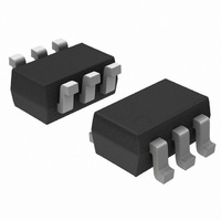
NTJD4158CT1G ON Semiconductor, NTJD4158CT1G Datasheet - Page 4

NTJD4158CT1G
Manufacturer Part Number
NTJD4158CT1G
Description
MOSFET N/P-CHAN COMPL SOT-363
Manufacturer
ON Semiconductor
Datasheet
1.NTJD4158CT2G.pdf
(7 pages)
Specifications of NTJD4158CT1G
Fet Type
N and P-Channel
Fet Feature
Logic Level Gate
Rds On (max) @ Id, Vgs
1.5 Ohm @ 10mA, 4.5V
Drain To Source Voltage (vdss)
30V, 20V
Current - Continuous Drain (id) @ 25° C
250mA, 880mA
Vgs(th) (max) @ Id
1.5V @ 100µA
Gate Charge (qg) @ Vgs
1.5nC @ 5V
Input Capacitance (ciss) @ Vds
33pF @ 5V
Power - Max
270mW
Mounting Type
Surface Mount
Package / Case
SC-70-6, SC-88, SOT-363
Lead Free Status / RoHS Status
Lead free / RoHS Compliant
Other names
NTJD4158CT1G
NTJD4158CT1GOSTR
NTJD4158CT1GOSTR
Available stocks
Company
Part Number
Manufacturer
Quantity
Price
Company:
Part Number:
NTJD4158CT1G
Manufacturer:
ON
Quantity:
30 000
Part Number:
NTJD4158CT1G
Manufacturer:
ON/安森美
Quantity:
20 000
GATE−TO−SOURCE OR DRAIN−TO−SOURCE VOLTAGE (VOLTS)
1000
100
50
40
30
20
10
10
0
10
1
Figure 9. Resistive Switching Time Variation
C
C
iss
rss
V
I
V
D
t
V
t
DD
GS
d(off)
d(on)
= 0.25 A
DS
5
t
t
= 5.0 V
= 4.5 V
r
f
= 0 V
Figure 7. Capacitance Variation
V
TYPICAL N−CHANNEL PERFORMANCE CURVES
R
GS
G
, GATE RESISTANCE (OHMS)
vs. Gate Resistance
0
V
V
GS
DS
= 0 V
5
10
10
15
T
J
20
= 25°C
http://onsemi.com
C
C
C
iss
oss
rss
100
25
4
0.08
0.06
0.04
0.02
0.1
0
5
4
3
2
1
0
0.5
0
Figure 10. Diode Forward Voltage vs. Current
V
T
Figure 8. Gate−to−Source Voltage vs. Total
V
GS
J
SD
(T
= 25°C
Q
GS
= 0 V
J
, SOURCE−TO−DRAIN VOLTAGE (VOLTS)
0.55
0.2
= 25°C unless otherwise noted)
Q
G
, TOTAL GATE CHARGE (nC)
Q
0.4
0.6
Gate Charge
GD
Q
G
0.65
0.6
0.8
0.7
I
T
D
J
= 0.1 A
= 25°C
0.75
1


