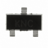
ZXMN2F30FHTA Diodes Zetex, ZXMN2F30FHTA Datasheet - Page 4

ZXMN2F30FHTA
Manufacturer Part Number
ZXMN2F30FHTA
Description
MOSFET N-CHAN 20V SOT23-3
Manufacturer
Diodes Zetex
Type
Power MOSFETr
Datasheet
1.ZXMN2F30FHTA.pdf
(8 pages)
Specifications of ZXMN2F30FHTA
Fet Type
MOSFET N-Channel, Metal Oxide
Fet Feature
Logic Level Gate
Rds On (max) @ Id, Vgs
45 mOhm @ 2.5A, 4.5V
Drain To Source Voltage (vdss)
20V
Current - Continuous Drain (id) @ 25° C
4.1A
Vgs(th) (max) @ Id
1.5V @ 250µA
Gate Charge (qg) @ Vgs
4.8nC @ 4.5V
Input Capacitance (ciss) @ Vds
452pF @ 10V
Power - Max
960mW
Mounting Type
Surface Mount
Package / Case
SOT-23-3, TO-236-3, Micro3™, SSD3, SST3
Number Of Elements
1
Polarity
N
Channel Mode
Enhancement
Drain-source On-res
0.045Ohm
Drain-source On-volt
20V
Gate-source Voltage (max)
±12V
Continuous Drain Current
4.9A
Power Dissipation
1.4W
Operating Temp Range
-55C to 150C
Operating Temperature Classification
Military
Mounting
Surface Mount
Pin Count
3
Package Type
SOT-23
Lead Free Status / RoHS Status
Lead free / RoHS Compliant
Other names
ZXMN2F30FHTR
Available stocks
Company
Part Number
Manufacturer
Quantity
Price
Company:
Part Number:
ZXMN2F30FHTA
Manufacturer:
Diodes
Quantity:
24 600
Part Number:
ZXMN2F30FHTA
Manufacturer:
ZETEX/DIODES
Quantity:
20 000
Part Number:
ZXMN2F30FHTA/KNC
Manufacturer:
ZETEX
Quantity:
20 000
Electrical characteristics (at T
(*) Measured under pulsed conditions. Pulse width ≤ 300µs; duty cycle ≤2%.
(†) For design aid only, not subject to production testing.
(‡) Switching characteristics are independent of operating junction temperature.
Issue 1 - January 2008
© Zetex Semiconductors plc 2008
NOTES:
Parameter
Static
Drain-Source Breakdown
Voltage
Zero Gate Voltage Drain
Current
Gate-Body Leakage
Gate-Source Threshold
Voltage
Static Drain-Source
On-State Resistance
Forward
Transconductance
Dynamic
Input Capacitance
Output Capacitance
Reverse Transfer
Capacitance
Switching
Turn-On-Delay Time
Rise Time
Turn-Off Delay Time
Fall Time
Total Gate Charge
Gate-Source Charge
Gate Drain Charge
Source-drain diode
Diode Forward Voltage
(†)
(‡)(†)
(*)(†)
(*)
(*)
V
I
V
R
g
C
C
C
t
t
t
Q
V
Symbol
I
t
Q
Q
DSS
GSS
d(on)
r
d(off)
f
fs
(BR)DSS
GS(th)
DS(on)
iss
oss
rss
SD
g
gs
gd
amb
Min.
0.6
= 25°C unless otherwise stated)
20
4
Typ.
19.4
10.2
0.75
452
102
0.9
8.6
2.9
5.6
4.8
1.2
58
1
0.045
0.065
Max.
100
1.5
1.2
1
Unit
nA
µA
nC
nC
nC
pF
pF
pF
ns
ns
ns
ns
Ω
Ω
V
V
S
V
ZXMN2F30FH
I
V
V
I
V
V
V
V
f=1MHz
V
I
R
V
I
I
Conditions
D
D
D
D
S
DS
GS
GS
GS
DS
DS
DD
G
DS
= 1.25A, V
= 250µA, V
= 250µA, V
= 1A
= 3.5A
≈ 6.0Ω
= 20V, V
= 10V, I
= 10V, V
= 10V, V
=±12V, V
= 4.5V, I
= 2.5V, I
= 10V, V
www.zetex.com
D
D
D
GS
GS
GS
GS
GS
= 3A
GS
DS
DS
= 2.5A
= 2.0A
=0V
=0V
= 4.5V
=0V
= 4.5V
=0V
=V
=0V
GS


