NMSD200B01-7 Diodes Inc, NMSD200B01-7 Datasheet - Page 6
NMSD200B01-7
Manufacturer Part Number
NMSD200B01-7
Description
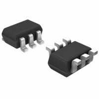
MOSFET N-CH 60V 200MA SOT363
Manufacturer
Diodes Inc
Datasheet
1.NMSD200B01-7.pdf
(8 pages)
Specifications of NMSD200B01-7
Fet Type
MOSFET N-Channel, Metal Oxide
Fet Feature
Diode (Isolated)
Rds On (max) @ Id, Vgs
3 Ohm @ 50mA, 5V
Drain To Source Voltage (vdss)
60V
Current - Continuous Drain (id) @ 25° C
200mA
Vgs(th) (max) @ Id
3V @ 1mA
Input Capacitance (ciss) @ Vds
50pF @ 25V
Power - Max
200mW
Mounting Type
Surface Mount
Package / Case
SC-70-6, SC-88, SOT-363
Lead Free Status / RoHS Status
Lead free / RoHS Compliant
Gate Charge (qg) @ Vgs
-
Other names
NMSD200B01DITR
NMSD200B01TR
NMSD200B01TR
NMSD200B01TR
NMSD200B01TR


ESD Protected N-MOSFET (DMN601K) and Schottky Barrier
Diode (SD103AWS) integrated as one in NMSD200B01 can be
used as a discrete entity for general applications or part of
circuits to function as a low side switch in a Synchronous
Rectifier. The N-MOSFET is selected based on the input
voltage range as the maximum duty cycles can be greater than
45%. Schottky diode is selected based on instantaneous V
(less than 0.75 V) at maximum operation current. The Schottky
diode dissipates very little power because it is on for only a
small portion of the switching cycle. Normally it shows much
lower leakage current and smaller on-resistance (R
compared to its monolithic counterpart. This device is designed
to improve efficiency and reliability of synchronous buck
converters used in voltage regulator modules (VRM). The
lower V
time the high side MOSFET is turned on in the buck converter,
the low side Schottky diode is forced to recover the stored
charge and there will be lower loss due to the lower Reverse
Recovery charge of the Schottky diode.
It is designed to replace a discrete N-MOSFET and a Schottky
diode in two separate packages into one small package as
shown in Fig. 17. The Schottky diode parallel to the MOSFET
body diode is faster and has lower voltage drop compared to
the integrated body diode. Overall this device consumes less
board space and also helps to minimize conduction or switching
losses due to parasitic inductances (e.g. PCB traces) in power
supply applications. (Please see Fig. 18 for one example of
typical application circuit used in conjunction with DC-DC
converter as a part of power management system and Fig. 19
for low side DC load control.)
Application Details
DS30911 Rev. 7 - 2
f
of the Schottky diode leads to lower static loss. Every
D C - D C C o n t r o l l e r
a n d D r i v e r I C S
Fig. 18 Synchronous Buck Converter with Integrated Schottky Diode
Typical Application Circuits
DS(ON)
D M N 6 0 1 K
H i g h S i d e
D M N 6 0 1 K
L o w S i d e
) even
Q 2
Q 1
f
www.diodes.com
N M S D 2 0 0 B 0 1
0
B o d y D i o d e
6 of 8
G a t e
D 1
S D 1 0 3 A W S
M a i n I n d u c t o r
D M N 6 0 1 K
0
V C C
Q 1
Fig. 17 Example Circuit Diagram
C 1
S o u r c e
D r a i n
L o a d
C a t h o d e
A n o d e
S D 1 0 3 A W S
D 1
© Diodes Incorporated
NMSD200B01
Related parts for NMSD200B01-7
Image
Part Number
Description
Manufacturer
Datasheet
Request
R

Part Number:
Description:
Diodes (General Purpose, Power, Switching) 240V 350mW
Manufacturer:
Diodes Inc
Datasheet:

Part Number:
Description:
Diodes (General Purpose, Power, Switching) -
Manufacturer:
Diodes Inc
Part Number:
Description:
Diodes (General Purpose, Power, Switching) -
Manufacturer:
Diodes Inc

Part Number:
Description:
Diodes (General Purpose, Power, Switching) NPN Small SIG 50V 45V VCEO 6.0V VEBO
Manufacturer:
Diodes Inc
Datasheet:
Part Number:
Description:
Diodes (General Purpose, Power, Switching) NPN Small SIG 30V 30V VCEO 5.0V VEBO
Manufacturer:
Diodes Inc
Datasheet:
Part Number:
Description:
Diodes (General Purpose, Power, Switching) NPN Small SIG -80V -65V VCEO -5.0 VEBO
Manufacturer:
Diodes Inc
Datasheet:
Part Number:
Description:
Diodes (General Purpose, Power, Switching) NPN Small SIG -50V -45V VCEO 6.0V VEBO
Manufacturer:
Diodes Inc
Part Number:
Description:
Diodes (General Purpose, Power, Switching) Dual Switching DIODE 100V Vrm 75Vrrm 53Vr
Manufacturer:
Diodes Inc
Datasheet:

Part Number:
Description:
Diodes (General Purpose, Power, Switching) Vr/80V Io/125mA T/R
Manufacturer:
Diodes Inc
Datasheet:

Part Number:
Description:
Diodes (General Purpose, Power, Switching) HV DUAL SW DIODE 300V
Manufacturer:
Diodes Inc
Datasheet:

Part Number:
Description:
Diodes (General Purpose, Power, Switching) 80V 150mW
Manufacturer:
Diodes Inc
Datasheet:
Part Number:
Description:
Diodes (General Purpose, Power, Switching) 75V 150mW
Manufacturer:
Diodes Inc
Datasheet:

Part Number:
Description:
Diodes (General Purpose, Power, Switching) 200MW 80V
Manufacturer:
Diodes Inc
Part Number:
Description:
Diodes (General Purpose, Power, Switching) 100V Io/150mA T/R INVALID P/N
Manufacturer:
Diodes Inc

Part Number:
Description:
Diodes (General Purpose, Power, Switching) 350MW 75V
Manufacturer:
Diodes Inc