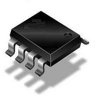
U4083B-MFPG3Y Atmel, U4083B-MFPG3Y Datasheet

U4083B-MFPG3Y
Specifications of U4083B-MFPG3Y
Available stocks
Related parts for U4083B-MFPG3Y
U4083B-MFPG3Y Summary of contents
Page 1
... The integrated circuit U4083B is a low-power audio amplifier for telephone loudspeak- ers. It has differential speaker outputs to maximize the output swing at low supply voltages. There is no need for coupler capacitors. The U4083B has an open-loop gain where the closed-loop gain is adjusted with two external resistors. A chip dis- able pin permits powering down and/or muting the input signal ...
Page 2
... Pin Symbol Function 1 CD Chip disable 2 FC2 Filtering, power supply rejection 3 FC1 Filtering, power supply rejection 4 V Amplifier input i 5 VO1 Amplifier output Voltage supply S 7 GND Ground 8 VO2 Amplifier output 2 U4083B VO2 2 7 GND FC2 V FC1 VO1 4655C–CORD–03/06 ...
Page 3
... IC disabled shows the power supply current diagram. The change in differential gain µs off , C and and, therefore, do not change when the U4083B S (Pin 5) and V (Pin 8), turn to a high impedance condition and ground. S and dominant at low frequencies 2 9). The values of C and C depend on the conditions of each application. ...
Page 4
... The right (descending) portion of each curve is defined by the maximum internal power dissipation of the IC at 25°C. At higher ambient temperatures, the maximum load power must be reduced according to the above men- tioned equation. U4083B 4 , Pin 5: Amplifier Output ...
Page 5
... Symbol Value – V 1.0 to +18 S – 1 – 1 ±250 T +140 j – +150 stg – +70 amb P 440 tot Symbol Value R 180 thJA Symbol Value 8.0 to 100 L I ±200 – +70 amb U4083B Unit °C °C °C mW Unit K/W Unit °C 5 ...
Page 6
... Output high level Output low level Output DC offset voltage (V – Input bias current Equivalent resistance at Pin 3 Equivalent resistance at Pin 2 Chip disable Pin 1 Input voltage low Input voltage high Input resistance Power supply current U4083B 6 Test Conditions V = 6.0V 1.0 kHz 3.0V < 10 6.0V < 10% S ...
Page 7
... V switching from Amplifier 1 — Open-loop Gain and Phase 100 Gain (kHz) Typical Change Units ±40 pA/ C +0.003 %/ C –2.5 µA/ C –0.03 µ µ µ (µF) 2 99.33 92.67 Phase 86.00 79.33 72.67 66.00 1000 100 U4083B 7 ...
Page 8
... Figure 8-3. Figure 8-4. Figure 8-5. U4083B 8 Differential Gain versus Frequency 150 Input 16 0.1 µ Frequency (kHz) Power Supply Rejection versus Frequency — > 1 µF C > 1 µ 0.1 µ 0.1 µ µ µ 0.1 1 0.1 1 Power Supply Rejection versus Frequency — C ...
Page 9
... µ 0.1 µ 0.1 1 Power Supply Rejection versus Frequency — > 5 µ µ 0.1 µ 0.1 1 Device Dissipation — 1200 1000 800 600 400 200 µ µF 100 10 f (kHz 100 10 f (kHz Ohm 120 150 180 (mW) L U4083B 9 ...
Page 10
... Figure 8-9. Figure 8-10. Device Dissipation — R Figure 8-11. Distortion versus Power — kHz, Delta – G U4083B 10 Device Dissipation — 1200 1000 800 600 400 200 100 = 32 L 1200 1000 800 600 400 200 100 200 Ohm Ohm 16V Ohm 100 ...
Page 11
... Figure 8-12. Distortion versus Power — kHz, Delta – G Figure 8-13. Distortion versus Power — kHz or 3 kHz, Delta – G 4655C–CORD–03/ Ohm Ohm 100 200 Ohm Ohm Ohm Limit 100 200 P O U4083B = kHz Delta Ohm Ohm Ohm Limit Ohm L 300 400 (mW kHz Delta Ohm Limit Ohm ...
Page 12
... Figure 8-14. Maximum Allowable Load Power Figure 8-15. Power-supply Current Figure 8-16. Small Signal Response U4083B 12 600 T = 25°C - Derate at higher temperature amb 500 400 300 16 Ohm 200 8 Ohm 100 ( ( µs/Div 4655C–CORD–03/06 ...
Page 13
... Figure 8-17. Large Signal Response Figure 8-18. V Figure 8-19. V 4655C–CORD–03/06 20µs/Div – V versus Load Current S OH 1.3 1.2 1.1 1.0 0.9 0 versus Load Current OL 2.0 1.6 1.2 0.8 0 U4083B 2V< V < 200 120 160 (mA > 200 120 160 (mA ...
Page 14
... Figure 8-20. Application Circuit 75k 0.1µF C1 FC3 C2 1µF FC2 5µF U4083B 14 4 Amp1 50k Amp2 125k 2 50k U4083B 10R R1B 6 VS C1B 5 VO1 8 C2B VO2 1 Bias circuit 10R R2B CD 7 GND 100nF 100nF 4655C–CORD–03/06 ...
Page 15
... Ordering Information Extended Type Number U4083B-MFPY U4083B-MFPG3Y 10. Package Information Package SO8 Dimensions in mm 4655C–CORD–03/06 Package Remarks SO8, Pb-free Tube SO8, Pb-free Taped and reeled 5.00 4.85 1.4 0.25 0.4 0.10 1.27 3. technical drawings according to DIN specifications 1 4 U4083B 5.2 4 ...
Page 16
... Disclaimer: The information in this document is provided in connection with Atmel products. No license, express or implied, by estoppel or otherwise, to any intellectual property right is granted by this document or in connection with the sale of Atmel products. EXCEPT AS SET FORTH IN ATMEL’S TERMS AND CONDI- TIONS OF SALE LOCATED ON ATMEL’S WEB SITE, ATMEL ASSUMES NO LIABILITY WHATSOEVER AND DISCLAIMS ANY EXPRESS, IMPLIED OR STATUTORY WARRANTY RELATING TO ITS PRODUCTS INCLUDING, BUT NOT LIMITED TO, THE IMPLIED WARRANTY OF MERCHANTABILITY, FITNESS FOR A PARTICULAR PURPOSE, OR NON-INFRINGEMENT ...


