IRLR014TRPBF Vishay, IRLR014TRPBF Datasheet

MOSFET N-CH 60V 7.7A DPAK

IRLR014TRPBF

Manufacturer Part Number
IRLR014TRPBF
Description
MOSFET N-CH 60V 7.7A DPAK
Manufacturer
Vishay
Datasheet

Specifications of IRLR014TRPBF

Fet Type
MOSFET N-Channel, Metal Oxide
Fet Feature
Logic Level Gate
Rds On (max) @ Id, Vgs
200 mOhm @ 4.6A, 5V
Drain To Source Voltage (vdss)
60V
Current - Continuous Drain (id) @ 25° C
7.7A
Vgs(th) (max) @ Id
2V @ 250µA
Gate Charge (qg) @ Vgs
8.4nC @ 5V
Input Capacitance (ciss) @ Vds
400pF @ 25V
Power - Max
2.5W
Mounting Type
Surface Mount
Package / Case
DPak, TO-252 (2 leads+tab), SC-63
Transistor Polarity
N Channel
Continuous Drain Current Id
7.7A
Drain Source Voltage Vds
60V
On Resistance Rds(on)
200mohm
Rds(on) Test Voltage Vgs
5V
Leaded Process Compatible
Yes
Configuration
Single
Resistance Drain-source Rds (on)
0.2 Ohms
Drain-source Breakdown Voltage
60 V
Gate-source Breakdown Voltage
+/- 10 V
Continuous Drain Current
7.7 A
Power Dissipation
2.5 W
Maximum Operating Temperature
+ 150 C
Mounting Style
SMD/SMT
Minimum Operating Temperature
- 55 C
Lead Free Status / RoHS Status
Lead free / RoHS Compliant
Lead Free Status / RoHS Status
Lead free / RoHS Compliant, Lead free / RoHS Compliant
Other names
IRLR014PBFTR

Available stocks

Company
Part Number
Manufacturer
Quantity
Price
Part Number:
IRLR014TRPBF
Manufacturer:
Microchip
Quantity:
168
Part Number:
IRLR014TRPBF
Manufacturer:
IR/VSHAY
Quantity:
20 000
Company:
Part Number:
IRLR014TRPBF
Quantity:
70 000
Note
a. See device orientation.
Notes
a. Repetitive rating; pulse width limited by maximum junction temperature (see fig. 11).
b. V
c. I
d. 1.6 mm from case.
e. When mounted on 1" square PCB (FR-4 or G-10 material).
* Pb containing terminations are not RoHS compliant, exemptions may apply
Document Number: 91321
S09-0058-Rev. A, 02-Feb-09
PRODUCT SUMMARY
V
R
Q
Q
Q
Configuration
ORDERING INFORMATION
Package
Lead (Pb)-free
SnPb
ABSOLUTE MAXIMUM RATINGS T
PARAMETER
Drain-Source Voltage
Gate-Source Voltage
Continuous Drain Current
Pulsed Drain Current
Linear Derating Factor
Linear Derating Factor (PCB Mount)
Single Pulse Avalanche Energy
Maximum Power Dissipation
Maximum Power Dissipation (PCB Mount)
Peak Diode Recovery dV/dt
Operating Junction and Storage Temperature Range
Soldering Recommendations (Peak Temperature)
(TO-252)
D
DS
DS(on)
g
gs
gd
SD
DPAK
DD
(Max.) (nC)
(nC)
(nC)
(V)
≤ 10 A, dI/dt ≤ 90 A/µs, V
= 25 V, starting T
(Ω)
G
S
D
(TO-251)
IPAK
a
J
= 25 °C, L = 924 µH, R
G
c
D S
DPAK (TO-252)
IRLR014PbF
SiHLR014-E3
IRLR014
SiHLR014
DD
b
V
≤ V
GS
e
= 5.0 V
DS
G
, T
J
N-Channel MOSFET
e
≤ 150 °C.
Single
8.4
3.5
6.0
60
G
= 25 Ω, I
D
S
C
Power MOSFET
V
= 25 °C, unless otherwise noted
0.20
IRLR014, IRLU014, SiHLR014, SiHLU014
GS
DPAK (TO-252)
IRLR014TRPbF
SiHLR014T-E3
IRLR014TR
SiHLR014T
AS
at 5.0 V
= 7.7 A (see fig. 12).
T
T
for 10 s
C
A
= 25 °C
= 25 °C
a
a
T
T
C
C
= 100 °C
a
= 25 °C
FEATURES
• Dynamic dV/dt Rating
• Surface Mount (IRLR014, SiHLR014)
• Straight Lead (IRLU014, SiHLU014)
• Available in Tape and Reel
• Logic-Level Gate Drive
• R
• Fast Switching
• Lead (Pb)-free Available
DESCRIPTION
Third generation Power MOSFETs from Vishay provide the
designer with the best combination of fast switching,
ruggedized
cost-effectiveness.
The DPAK is designed for surface mounting using vapor
phase, infrared, or wave soldering techniques. The straight
lead version (IRLU, SiHLU series) is for through-hole
mounting applications. Power dissipation levels up to 1.5 W
are possible in typical surface mount applications.
a
DS(on)
Specified at V
SYMBOL
DPAK (TO-252)
IRLR014TRLPbF
SiHLR014TL-E3
IRLR014TRL
SiHLR014TL
T
dV/dt
J
V
V
E
I
P
, T
device
I
DM
DS
GS
AS
D
D
stg
a
a
design,
GS
a
a
= 4 V and 5 V
- 55 to + 150
LIMIT
0.020
260
± 10
0.20
7.7
4.9
2.5
4.5
60
31
47
25
low
Vishay Siliconix
d
IPAK (TO-251)
IRLU014PbF
SiHLU014-E3
IRLU014
SiHLU014
on-resistance
www.vishay.com
UNIT
W/°C
V/ns
RoHS*
COMPLIANT
mJ
°C
W
V
A
Available
and
1

Related parts for IRLR014TRPBF

IRLR014TRPBF Summary of contents

Page 1

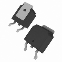
... The DPAK is designed for surface mounting using vapor S phase, infrared, or wave soldering techniques. The straight N-Channel MOSFET lead version (IRLU, SiHLU series) is for through-hole mounting applications. Power dissipation levels up to 1.5 W are possible in typical surface mount applications. DPAK (TO-252) a IRLR014TRPbF a SiHLR014T-E3 a IRLR014TR a SiHLR014T = 25 °C, unless otherwise noted ° ...

Page 2

... IRLR014, IRLU014, SiHLR014, SiHLU014 Vishay Siliconix THERMAL RESISTANCE RATINGS PARAMETER Maximum Junction-to-Ambient Maximum Junction-to-Ambient a (PCB Mount) Maximum Junction-to-Case (Drain) Note a. When mounted on 1" square PCB (FR-4 or G-10 material). SPECIFICATIONS °C, unless otherwise noted J PARAMETER Static Drain-Source Breakdown Voltage V Temperature Coefficient DS Gate-Source Threshold Voltage ...

Page 3

... TYPICAL CHARACTERISTICS 25 °C, unless otherwise noted Fig Typical Output Characteristics, T Fig Typical Output Characteristics, T Document Number: 91321 S09-0058-Rev. A, 02-Feb-09 IRLR014, IRLU014, SiHLR014, SiHLU014 = 25 °C Fig Typical Transfer Characteristics C = 150 °C Fig Normalized On-Resistance vs. Temperature C Vishay Siliconix www.vishay.com 3 ...

Page 4

... IRLR014, IRLU014, SiHLR014, SiHLU014 Vishay Siliconix Fig Typical Capacitance vs. Drain-to-Source Voltage Fig Typical Gate Charge vs. Gate-to-Source Voltage www.vishay.com 4 Fig Typical Source-Drain Diode Forward Voltage Fig Maximum Safe Operating Area Document Number: 91321 S09-0058-Rev. A, 02-Feb-09 ...

Page 5

... Fig Maximum Effective Transient Thermal Impedance, Junction-to-Case Document Number: 91321 S09-0058-Rev. A, 02-Feb-09 IRLR014, IRLU014, SiHLR014, SiHLU014 Pulse width ≤ 1 µs Duty factor ≤ 0.1 % Fig. 10a - Switching Time Test Circuit d(on) Fig. 10b - Switching Time Waveforms Vishay Siliconix D.U. d(off) f www.vishay.com 5 ...

Page 6

... IRLR014, IRLU014, SiHLR014, SiHLU014 Vishay Siliconix Vary t to obtain p required I AS D.U 0.01 Ω Fig. 12a - Unclamped Inductive Test Circuit Charge Fig. 13a - Basic Gate Charge Waveform www.vishay.com Fig. 12b - Unclamped Inductive Waveforms Fig. 12c - Maximum Avalanche Energy vs. Drain Current V DS ...

Page 7

... V GS Vishay Siliconix maintains worldwide manufacturing capability. Products may be manufactured at one of several qualified locations. Reliability data for Silicon Technology and Package Reliability represent a composite of all qualified locations. For related documents such as package/tape drawings, part marking, and reliability data, see www.vishay.com/ppg?91321. Document Number: 91321 S09-0058-Rev ...

Page 8

... Vishay disclaims any and all liability arising out of the use or application of any product described herein or of any information provided herein to the maximum extent permitted by law. The product specifications do not expand or otherwise modify Vishay’ ...

Related keywords