NJU6356EM-TE2 NJR, NJU6356EM-TE2 Datasheet
NJU6356EM-TE2
Specifications of NJU6356EM-TE2
Available stocks


Related parts for NJU6356EM-TE2


NJU6356EM-TE2 Summary of contents
Page 1
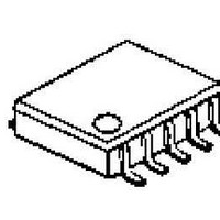
... Output Data Timer Counter Days of Sec. Min. Hr. Day W eek Days of Sec. Min. Hr. Day W eek Shift Register C ontroller & Clock Counter NJU6356 PACKAGE OUTLINE NJU6356ED NJU6356EM PIN CONFIGURATION I DATA XT CLK Oscillation Capacitor Cd=21pF / Cg=21pF on Chip Month Year Month Year DD DATA I/O CLK ...
Page 2
NJU6356 TREMINAL DESCRIPTION No. SYMBOL I/O Input/Output Select Terminal for DATA Terminal 1 "H" : Input, "L" : Output During the CE terminal is "L", the DATA terminal is high impedance Quartz Crystal Connecting Terminal (f=32.768kHz) Refer to ...
Page 3
Timer Data Reading When the I/O termianl is "L" and the CE tarminal is "H", timer data can read out. The output is LSB first and the output data strings is shown below. The timer data is transferred from ...
Page 4
NJU6356 3. Timer Data Writing When both of the I/O terminal and the CE terminal are "H", update is stopped, the oscillator divider is cleared, and the timer data can be written to the NJU6356. The timer data is written ...
Page 5
ABSOLUTE MAXIMUM RATINGS PARAMETER Supply Voltage Input Voltage Power Dissipation Operating Temperature Range Storage Temperature Range ELECTRICAL CHARACTERISTICS DC Characteristics PARAMETER Operating Current Low Battery Detect Voltage PARAMETER Operating Voltage Operating Current 3-st. Leakage Current Input Leakage Current Input Current ...
Page 6
NJU6356 CLK I (in) t WDS CLK 80% Input Data 20% APPLICATION CIRCUIT Main Power Supply - 6 - CLK I/O DH (out CLK 80% 20% Vss t WDH ...