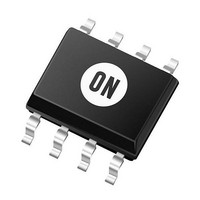
MC100EL32DR2 ON Semiconductor, MC100EL32DR2 Datasheet - Page 3

MC100EL32DR2
Manufacturer Part Number
MC100EL32DR2
Description
Clock Drivers & Distribution 5V ECL Divide
Manufacturer
ON Semiconductor
Datasheet
1.MC100EL32DR2.pdf
(9 pages)
Specifications of MC100EL32DR2
Mounting Style
SMD/SMT
Package / Case
SOIC-8
Lead Free Status / RoHS Status
Lead free / RoHS Compliant
NOTE: Device will meet the specifications after thermal equilibrium has been established when mounted in a test socket or printed circuit
2. Input and output parameters vary 1:1 with V
3. Outputs are terminated through a 50 W resistor to V
4. V
NOTE: Device will meet the specifications after thermal equilibrium has been established when mounted in a test socket or printed circuit
5. Input and output parameters vary 1:1 with V
6. Outputs are terminated through a 50 W resistor to V
7. V
Table 3. 10EL SERIES PECL DC CHARACTERISTICS
Table 4. 10EL SERIES NECL DC CHARACTERISTICS
Symbol
Symbol
I
V
V
V
V
V
V
I
I
I
V
V
V
V
V
V
I
I
EE
IH
IL
EE
IH
IL
OH
OL
IH
IL
BB
IHCMR
OH
OL
IH
IL
BB
IHCMR
signal. Normal operation is obtained if the HIGH level falls within the specified range and the peak-to-peak voltage lies between V
signal. Normal operation is obtained if the HIGH level falls within the specified range and the peak-to-peak voltage lies between V
IHCMR
IHCMR
board with maintained transverse airflow greater than 500 lfpm. Electrical parameters are guaranteed only over the declared
operating temperature range. Functional operation of the device exceeding these conditions is not implied. Device specification limit
values are applied individually under normal operating conditions and not valid simultaneously.
min varies 1:1 with V
min varies 1:1 with V
Power Supply Current
Output HIGH Voltage (Note 6)
Output LOW Voltage (Note 3)
Input HIGH Voltage (Single−Ended)
Input LOW Voltage (Single−Ended)
Output Voltage Reference
Input HIGH Voltage Common Mode
Range (Differential Configuration) (Note 4)
Input HIGH Current
Input LOW Current
Power Supply Current
Output HIGH Voltage (Note 6)
Output LOW Voltage (Note 6)
Input HIGH Voltage (Single−Ended)
Input LOW Voltage (Single−Ended)
Output Voltage Reference
Input HIGH Voltage Common Mode
Range (Differential Configuration)
(Note 7)
Input HIGH Current
Input LOW Current
Characteristic
Characteristic
EE
EE
, V
, V
IHCMR
IHCMR
max varies 1:1 with V
max varies 1:1 with V
CC
CC
. V
. V
EE
EE
CC
CC
can vary +0.25 V / −0.5 V.
can vary +0.25 V / −0.5 V.
−1080
−1950
−1230
−1950
−1.43
−2.5
Min
0.5
− 2.0 V.
− 2.0 V.
3920
3050
3770
3050
3.57
Min
2.5
0.5
http://onsemi.com
−40°C
−1800
CC
CC
−990
Typ
25
. The V
. The V
V
V
−40°C
4010
3200
CC
CC
Typ
25
3
= 5.0 V; V
= 0 V; V
−1650
−1500
IHCMR
−1.30
IHCMR
−890
−890
Max
−0.4
150
30
4110
3350
4110
3500
Max
150
3.7
4.6
30
range is referenced to the most positive side of the differential input
range is referenced to the most positive side of the differential input
EE
EE
−1950
−1950
−1130
−1.35
−980
−2.5
Min
0.5
= −5.0 V (Note 5)
= 0 V (Note 2)
4020
3050
3870
3050
3.65
Min
2.5
0.5
−1790
25°C
−895
Typ
25
25°C
4105
3210
Typ
25
−1630
−1480
−1.25
−810
−810
Max
−0.4
150
30
4190
3370
4190
3520
Max
3.75
150
4.6
30
−1950
−1060
−1950
−1.31
−910
−2.5
Min
0.3
4090
3050
3940
3050
3.69
Min
2.5
0.3
−1773
85°C
−815
Typ
85°C
4185
3227
25
Typ
25
PP
PP
−1595
−1445
−1.19
−720
−720
4280
3405
4280
3555
Max
−0.4
Max
min and 1 V.
min and 1 V.
3.81
150
150
4.6
30
30
Unit
Unit
mA
mV
mV
mV
mV
mA
mV
mV
mV
mV
mA
mA
mA
mA
V
V
V
V


