MC100LVEP111FAR2 ON Semiconductor, MC100LVEP111FAR2 Datasheet - Page 2
MC100LVEP111FAR2
Manufacturer Part Number
MC100LVEP111FAR2
Description
Clock Drivers & Distribution 2.5V/3.3V 1:10 Diff
Manufacturer
ON Semiconductor
Type
ECL, HSTL, PECLr
Datasheet
1.MC100LVEP111FA.pdf
(13 pages)
Specifications of MC100LVEP111FAR2
Minimum Operating Temperature
- 40 C
Mounting Style
SMD/SMT
Multiply / Divide Factor
2:1
Number Of Clock Inputs
2
Output Logic Level
ECL, PECL
Supply Voltage (max)
+/- 3.8 V
Supply Voltage (min)
+/- 2.375 V
Maximum Operating Temperature
+ 85 C
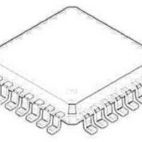
Package / Case
LQFP-32
Lead Free Status / RoHS Status
Lead free / RoHS Compliant


V
V
Q2
Q2
Q1
Q1
Q0
Q0
CC
CC
Warning: All V
to Power Supply to guarantee proper operation.
25
26
27
28
29
30
31
32
Figure 1. LQFP−32 Pinout (Top View)
V
Q3
24
CC
1
CC
Q3
23
2
and V
Q4
22
3
MC100LVEP111
EE
CLK_SEL
Q4
21
pins must be externally connected
4
CLK0
CLK0
CLK1
CLK1
V
V
V
V
Q5
20
CC
BB
EE
5
BB
Q5
19
1
2
3
4
5
6
7
8
6
V
Figure 2. QFN−32 Pinout (Top View)
V
CC
32
Q6
CC
18
9
7
Q9
V
Q0
10
31
Q6
17
8
EE
http://onsemi.com
Q9
16
15
14
13
12
10
11
MC100LVEP111
9
Q0
30
11
Q8
Q1
12
29
2
V
Q7
Q7
Q8
Q8
Q9
Q9
V
Q8
Q1
CC
CC
13
28
Q7
Table 2. FUNCTION TABLE
Table 1. PIN DESCRIPTION
Q2
14
* Pins will default LOW when left open.
** Pins will default to 2/3V
27
CLK0*, CLK0**
CLK1*, CLK1**
Q0:9, Q0:9
CLK_SEL*
V
V
V
EP
PIN
BB
CC
EE
Q7
Q2 V
15
CLK_SEL
26
V
H
L
16
CC
25
CC
24
23
22
21
20
19
18
17
Exposed Pad (EP)
Q3
Q3
Q4
Q4
Q5
Q5
Q6
Q6
FUNCTION
ECL/PECL/HSTL CLK Input
ECL/PECL/HSTL CLK Input
ECL/PECL Outputs
ECL/PECL Active Clock Select Input
Reference Voltage Output
Positive Supply
Negative Supply
The exposed pad (EP) on the package
bottom must be attached to a heat−sink-
ing conduit. The exposed pad may only
be electrically connected to V
CC
when left open.
Active Input
CLK0, CLK0
CLK1, CLK1
EE
.
Related parts for MC100LVEP111FAR2
Image
Part Number
Description
Manufacturer
Datasheet
Request
R

Part Number:
Description:
ON Semiconductor [VOLTAGE REGULATOR]
Manufacturer:
ON Semiconductor
Datasheet:
Part Number:
Description:
357-036-542-201 CARDEDGE 36POS DL .156 BLK LOPRO
Manufacturer:
ON Semiconductor
Datasheet:
Part Number:
Description:
357-036-542-201 CARDEDGE 36POS DL .156 BLK LOPRO
Manufacturer:
ON Semiconductor
Datasheet:
Part Number:
Description:
357-036-542-201 CARDEDGE 36POS DL .156 BLK LOPRO
Manufacturer:
ON Semiconductor
Datasheet:
Part Number:
Description:
357-036-542-201 CARDEDGE 36POS DL .156 BLK LOPRO
Manufacturer:
ON Semiconductor
Datasheet:
Part Number:
Description:
357-036-542-201 CARDEDGE 36POS DL .156 BLK LOPRO
Manufacturer:
ON Semiconductor
Datasheet:
Part Number:
Description:
357-036-542-201 CARDEDGE 36POS DL .156 BLK LOPRO
Manufacturer:
ON Semiconductor
Datasheet:
Part Number:
Description:
357-036-542-201 CARDEDGE 36POS DL .156 BLK LOPRO
Manufacturer:
ON Semiconductor
Datasheet:
Part Number:
Description:
357-036-542-201 CARDEDGE 36POS DL .156 BLK LOPRO
Manufacturer:
ON Semiconductor
Datasheet:
Part Number:
Description:
357-036-542-201 CARDEDGE 36POS DL .156 BLK LOPRO
Manufacturer:
ON Semiconductor
Datasheet:
Part Number:
Description:
357-036-542-201 CARDEDGE 36POS DL .156 BLK LOPRO
Manufacturer:
ON Semiconductor
Datasheet:
Part Number:
Description:
Manufacturer:
ON Semiconductor
Datasheet:
Part Number:
Description:
Manufacturer:
ON Semiconductor
Datasheet:
Part Number:
Description:
Manufacturer:
ON Semiconductor
Datasheet: