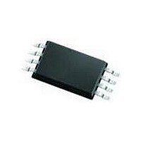
MC100EP33DT ON Semiconductor, MC100EP33DT Datasheet

MC100EP33DT
Specifications of MC100EP33DT
Available stocks
Related parts for MC100EP33DT
MC100EP33DT Summary of contents
Page 1
MC10EP33, MC100EP33 3.3V / 5V ECL B4 Divider Description The MC10/100EP33 is an integrated B4 divider. The differential clock inputs. The V pin, an internally generated voltage supply, is available to BB this device only. For single-ended input conditions, the unused ...
Page 2
RESET 1 R CLK 2 B4 CLK Figure 1. 8−Lead Pinout (Top View) and Logic Diagram CLK RESET Q Table 3. ATTRIBUTES Internal Input Pulldown Resistor Internal Input Pullup Resistor ESD Protection Moisture Sensitivity, Indefinite Time ...
Page 3
Table 4. MAXIMUM RATINGS Symbol Parameter V PECL Mode Power Supply CC V NECL Mode Power Supply EE V PECL Mode Input Voltage I NECL Mode Input Voltage I Output Current out I V Sink/Source Operating Temperature ...
Page 4
Table 6. 10EP DC CHARACTERISTICS, PECL Symbol Characteristic I Power Supply Current EE V Output HIGH Voltage (Note Output LOW Voltage (Note Input HIGH Voltage (Single−Ended Input LOW Voltage (Single−Ended ...
Page 5
Table 8. 100EP DC CHARACTERISTICS, PECL Symbol Characteristic I Power Supply Current EE V Output HIGH Voltage (Note 13 Output LOW Voltage (Note 13 Input HIGH Voltage (Single−Ended Input LOW Voltage (Single−Ended ...
Page 6
Table 10. 100EP DC CHARACTERISTICS, NECL Symbol Characteristic I Power Supply Current EE V Output HIGH Voltage (Note 19 Output LOW Voltage (Note 19 Input HIGH Voltage (Single−Ended Input LOW Voltage (Single−Ended ...
Page 7
INPUT FREQUENCY (MHz) in Figure 3. Input Frequency ( Driver Device ...
Page 8
... MC10EP33MNR4 MC10EP33MNR4G MC100EP33D MC100EP33DG MC100EP33DR2 MC100EP33DR2G MC100EP33DT MC100EP33DTG MC100EP33DTR2 MC100EP33DTR2G MC100EP33MNR4 MC100EP33MNR4G †For information on tape and reel specifications, including part orientation and tape sizes, please refer to our Tape and Reel Packaging Specifications Brochure, BRD8011/D. Resource Reference of Application Notes AN1405/D AN1406/D AN1503/D ...
Page 9
... G C SEATING PLANE −Z− 0.25 (0.010 *For additional information on our Pb−Free strategy and soldering details, please download the ON Semiconductor Soldering and Mounting Techniques Reference Manual, SOLDERRM/D. PACKAGE DIMENSIONS SOIC−8 NB CASE 751−07 ISSUE 0.10 (0.004 SOLDERING FOOTPRINT* 1 ...
Page 10
K 8x REF 0.10 (0.004) 0.15 (0.006 L −U− PIN 1 IDENT 0.15 (0.006 −V− C 0.10 (0.004) D −T− G SEATING PLANE PACKAGE DIMENSIONS TSSOP−8 ...
Page 11
... Opportunity/Affirmative Action Employer. This literature is subject to all applicable copyright laws and is not for resale in any manner. PUBLICATION ORDERING INFORMATION LITERATURE FULFILLMENT: Literature Distribution Center for ON Semiconductor P.O. Box 5163, Denver, Colorado 80217 USA Phone: 303−675−2175 or 800−344−3860 Toll Free USA/Canada Fax: 303− ...


