MC100EL33D ON Semiconductor, MC100EL33D Datasheet
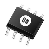
Clock Drivers & Distribution 5V ECL Divide

MC100EL33D

Manufacturer Part Number
MC100EL33D
Description
Clock Drivers & Distribution 5V ECL Divide
Manufacturer
ON Semiconductor
Datasheet

Specifications of MC100EL33D

Mounting Style
SMD/SMT
Package / Case
SOIC-8
Lead Free Status / RoHS Status
Lead free / RoHS Compliant

Available stocks

Company
Part Number
Manufacturer
Quantity
Price
Part Number:
MC100EL33D
Manufacturer:
MOTOROLA/摩托罗拉
Quantity:
20 000
Part Number:
MC100EL33D
Quantity:
170
Part Number:
MC100EL33DG
Manufacturer:
ON Semiconductor
Quantity:
186
Part Number:
MC100EL33DR2
Manufacturer:
MOTOROLA/摩托罗拉
Quantity:
20 000
Part Number:
MC100EL33DR2
Manufacturer:
ON
Quantity:
16 688
Company:
Part Number:
MC100EL33DR2G
Quantity:
1 750
Company:
Part Number:
MC100EL33DR2G
Quantity:
1 750
Part Number:
MC100EL33DTG
Manufacturer:
ON Semiconductor
Quantity:
135
Company:
Part Number:
MC100EL33DTG
Quantity:
24
MC10EL33, MC100EL33
5V ECL ÷4 Divider
Description
clock inputs and the V
interface to the device. The V
supply, is available to this device only. For single-ended input conditions,
the unused differential input is connected to V
voltage. V
V
to 0.5 mA. When not used, V
power-up, the internal flip-flops will attain a random state; the reset allows
for the synchronization of multiple EL33’s in a system.
Features
© Semiconductor Components Industries, LLC, 2008
August, 2008 − Rev. 10
BB
The MC10EL/100EL33 is an integrated ÷4 divider. The differential
The reset pin is asynchronous and is asserted on the rising edge. Upon
The 100 Series contains temperature compensation.
NECL Mode Operating Range: V
For Additional Information, see Application Note AND8003/D
Oxygen Index: 28 to 34
650 ps Propagation Delay
4.0 GHz Toggle Frequency
ESD Protection:
PECL Mode Operating Range: V
Internal Input Pulldown Resistors on CLK(s) and R.
Meets or Exceeds JEDEC Spec EIA/JESD78 IC Latchup Test
Moisture Sensitivity Level 1
Flammability Rating: UL 94 V−0 @ 0.125 in,
Transistor Count = 95 devices
Pb−Free Packages are Available
Figure 1. Logic Diagram and Pinout Assignment
and V
Reset
CLK
CLK
V
BB
BB
CC
may also rebias AC coupled inputs. When used, decouple
via a 0.01 mF capacitor and limit current sourcing or sinking
1
2
3
4
BB
Human Body Model; > 1 kV,
Machine Model; > 100 V
allow a differential, single-ended or AC coupled
BB
÷4
should be left open.
BB
R
CC
pin, an internally generated voltage
CC
= 0 V with V
= 4.2 V to 5.7 V with V
8
7
6
5
BB
as a switching reference
V
Q
Q
V
CC
EE
EE
= −4.2 V to −5.7 V
1
EE
= 0 V
See detailed ordering and shipping information in the package
dimensions section on page 7 of this data sheet.
H = MC10
K = MC100
4V = MC10
2K = MC100
A = Assembly Location
CASE 506AA
CASE 948R
MN SUFFIX
*For additional marking information, refer to
DT SUFFIX
CASE 751
D SUFFIX
TSSOP−8
8
(Note: Microdot may be in either location)
Application Note AND8002/D.
SOIC−8
8
DFN8
ORDERING INFORMATION
1
1
http://onsemi.com
8
1
8
1
HEL33
ALYWG
ALYW
Publication Order Number:
HL33
L = Wafer Lot
Y = Year
W = Work Week
M = Date Code
G = Pb−Free Package
1
DIAGRAMS*
G
G
MARKING
4
8
1
8
1
MC10EL33/D
ALYWG
1
KEL33
ALYW
KL33
G
G
4

Related parts for MC100EL33D

MC100EL33D Summary of contents

Page 1

MC10EL33, MC100EL33 5V ECL ÷4 Divider Description The MC10EL/100EL33 is an integrated ÷4 divider. The differential clock inputs and the V allow a differential, single-ended or AC coupled BB interface to the device. The V pin, an internally generated voltage BB ...

Page 2

Table 1. PIN DESCRIPTION Pin CLK, CLK ECL Clock Inputs* Reset ECL Asynch Reset ECL Data Outputs V Reference Voltage Output BB V Positive Supply CC V Negative Supply EE EP (DFN8 only) Thermal exposed pad must be ...

Page 3

Table 3. 10EL SERIES PECL DC CHARACTERISTICS Symbol Characteristic I Power Supply Current EE V Output HIGH Voltage (Note Output LOW Voltage (Note Input HIGH Voltage (Single−Ended Input LOW Voltage (Single−Ended) IL ...

Page 4

Table 5. 100EL SERIES PECL DC CHARACTERISTICS Symbol Characteristic I Power Supply Current EE V Output HIGH Voltage (Note Output LOW Voltage (Note Input HIGH Voltage (Single−Ended Input LOW Voltage (Single−Ended) IL ...

Page 5

Table 7. AC CHARACTERISTICS V CC Symbol Characteristic f Maximum Toggle Frequency max t Propagation Delay PLH t CLK to Q PHL Reset Set/Reset Recovery RR V Input Swing (Note 15 Cycle−to−Cycle Jitter JITTER t ...

Page 6

Resource Reference of Application Notes AN1405/D − ECL Clock Distribution Techniques AN1406/D − Designing with PECL (ECL at +5.0 V) AN1503/D − ECLinPSt I/O SPiCE Modeling Kit AN1504/D − Metastability and the ECLinPS Family AN1568/D − Interfacing Between LVDS and ...

Page 7

... MC10EL33DTR2 MC10EL33DTR2G MC10EL33MNR4 MC10EL33MNR4G MC100EL33D MC100EL33DG MC100EL33DR2 MC100EL33DR2G MC100EL33DT MC100EL33DTG MC100EL33DTR2 MC100EL33DTR2G MC100EL33MNR4 MC100EL33MNR4G †For information on tape and reel specifications, including part orientation and tape sizes, please refer to our Tape and Reel Packaging Specifications Brochure, BRD8011/D. Package SOIC−8 SOIC−8 (Pb− ...

Page 8

... G C SEATING PLANE −Z− 0.25 (0.010 *For additional information on our Pb−Free strategy and soldering details, please download the ON Semiconductor Soldering and Mounting Techniques Reference Manual, SOLDERRM/D. PACKAGE DIMENSIONS SOIC−8 NB CASE 751−07 ISSUE 0.10 (0.004 SOLDERING FOOTPRINT* 1 ...

Page 9

K 8x REF 0.10 (0.004) 0.15 (0.006 L −U− PIN 1 IDENT 0.15 (0.006 −V− C 0.10 (0.004) D −T− G SEATING PLANE PACKAGE DIMENSIONS TSSOP−8 ...

Page 10

... Opportunity/Affirmative Action Employer. This literature is subject to all applicable copyright laws and is not for resale in any manner. PUBLICATION ORDERING INFORMATION LITERATURE FULFILLMENT: Literature Distribution Center for ON Semiconductor P.O. Box 5163, Denver, Colorado 80217 USA Phone: 303−675−2175 or 800−344−3860 Toll Free USA/Canada Fax: 303− ...

Related keywords