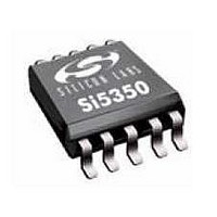
Si5350A-A-GT Silicon Laboratories Inc, Si5350A-A-GT Datasheet - Page 10

Si5350A-A-GT
Manufacturer Part Number
Si5350A-A-GT
Description
Clock Generators & Support Products Any-Rate Dual PLL 125MHz Clk 3 outputs
Manufacturer
Silicon Laboratories Inc
Type
Any Frequency CMOS Clock Generatorr
Datasheet
1.SI5350A-A-GM.pdf
(20 pages)
Specifications of Si5350A-A-GT
Mounting Style
SMD/SMT
Max Input Freq
0.008 MHz
Max Output Freq
125 MHz
Number Of Outputs
3
Operating Supply Voltage
3.3 V
Operating Temperature Range
- 40 C to + 85 C
Supply Current
20 mA
Package / Case
MSOP-10
Lead Free Status / RoHS Status
Lead free / RoHS Compliant
Si5350A
4.2.3. Invert/Non-Invert
By default, each of the output clocks are generated in phase (non-inverted) with respect to each other. An option to
invert any of the clock outputs is also available.
4.2.4. Output State When Disabled
There are up to three output enable pins configurable on the Si5350A as described in “4.3.4. Output Enable
(OEB_0, OEB_1, OEB_2)” . The output state when disabled for each of the outputs is configurable as one of the
following: disable low, disable high, or disable in high-impedance.
4.2.5. Powering Down Unused Outputs
Unused clock outputs can be completely powered down to conserve power.
4.3. Programmable Control Pins (P0–P4) Options
Up to five programmable control pins (P0-P4) are configurable allowing direct pin control of the following features:
4.3.1. Spread Spectrum Enable (SSEN)
An optional control pin allows disabling the spread spectrum feature for all outputs that were configured with
spread spectrum enabled. Hold SSEN low to disable spread spectrum. The SSEN pin provides a convenient
method of evaluating the effect of using spread spectrum clocks during EMI compliance testing.
4.3.2. Power Down (PDN)
An optional power down control pin allows a full shutdown of the Si5350A to minimize power consumption when its
output clocks are not being used. The Si5350A is in normal operation when the PDN pin is held low and is in power
down mode when held high. Power consumption when the device is in power down mode is indicated in Table 3 on
page 4.
4.3.3. Frequency Select (FS_0, FS_1)
The Si5350A offers the option of configuring up to two frequencies per clock output on CLK0-CLK5. This is a useful
feature for applications that need to support more than one clock rate on the same output. An example of this is
shown in Figure 5 where the FS pins selects which frequency is generated from the clock output: F1_0 is
generated when FS is set low, and F2_0 is generated when FS is set high.
10
Figure 5. Example of Generating Two Clock Frequencies from the Same Clock Output
Bit Level
FS0
0
1
Output Frequency Selected
F1_0:
F2_0:
Frequency
Am plitude
C enter
Figure 4. Available Spread Spectrum Profiles
74.25 MHz
74.25
1.001
N o Spread
Spectrum
f
MHz
c
FS0
Am plitude
R educed
and E M I
Rev. 0.2
XA
Si5350A
27 MHz
D ow n S pread
XB
CLK0
f
c
- 0.5% to - 2.5%
Spread A m ount
74.25
74.25
1.001
or
MHz
MHz
Processor
Video


