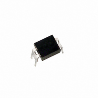
IRFD123PBF Vishay, IRFD123PBF Datasheet - Page 6

IRFD123PBF
Manufacturer Part Number
IRFD123PBF
Description
MOSFET N-CH 100V 1.3A 4-DIP
Manufacturer
Vishay
Datasheet
1.IRFD123PBF.pdf
(8 pages)
Specifications of IRFD123PBF
Transistor Polarity
N-Channel
Fet Type
MOSFET N-Channel, Metal Oxide
Fet Feature
Standard
Rds On (max) @ Id, Vgs
270 mOhm @ 780mA, 10V
Drain To Source Voltage (vdss)
100V
Current - Continuous Drain (id) @ 25° C
1.3A
Vgs(th) (max) @ Id
4V @ 250µA
Gate Charge (qg) @ Vgs
16nC @ 10V
Input Capacitance (ciss) @ Vds
360pF @ 25V
Power - Max
1.3W
Mounting Type
Through Hole
Package / Case
4-DIP (0.300", 7.62mm)
Minimum Operating Temperature
- 55 C
Configuration
Single Dual Drain
Resistance Drain-source Rds (on)
1.5 Ohm @ 10 V
Drain-source Breakdown Voltage
200 V
Gate-source Breakdown Voltage
+/- 20 V
Continuous Drain Current
0.6 A
Power Dissipation
1000 mW
Maximum Operating Temperature
+ 175 C
Mounting Style
Through Hole
Continuous Drain Current Id
1.3A
Drain Source Voltage Vds
100V
On Resistance Rds(on)
270mohm
Rds(on) Test Voltage Vgs
10V
Power Dissipation Pd
1.3W
No. Of Pins
4
Lead Free Status / RoHS Status
Lead free / RoHS Compliant
Lead Free Status / RoHS Status
Lead free / RoHS Compliant, Lead free / RoHS Compliant
Other names
*IRFD123PBF
IRFD123, SiHFD123
Vishay Siliconix
www.vishay.com
6
Vary t
required I
p
Fig. 12a - Unclamped Inductive Test Circuit
to obtain
10 V
Fig. 13a - Basic Gate Charge Waveform
AS
V
G
R
10 V
g
Q
GS
V
DS
t
p
Charge
Q
Q
GD
G
I
AS
D.U.T.
0.01 Ω
L
Fig. 12c - Maximum Avalanche Energy vs. Drain Current
+
-
V
DD
Fig. 12b - Unclamped Inductive Waveforms
V
I
AS
12 V
DS
Fig. 13b - Gate Charge Test Circuit
V
GS
Same type as D.U.T.
Current regulator
0.2 µF
Current sampling resistors
3 mA
50 kΩ
0.3 µF
t
p
I
G
S10-2466-Rev. C, 25-Oct-10
Document Number: 90161
D.U.T.
V
I
D
DS
+
-
V
V
DD
DS


