IRFU3410PBF International Rectifier, IRFU3410PBF Datasheet

MOSFET N-CH 100V 31A I-PAK

IRFU3410PBF

Manufacturer Part Number
IRFU3410PBF
Description
MOSFET N-CH 100V 31A I-PAK
Manufacturer
International Rectifier
Series
HEXFET®r
Datasheet

Specifications of IRFU3410PBF

Fet Type
MOSFET N-Channel, Metal Oxide
Fet Feature
Standard
Rds On (max) @ Id, Vgs
39 mOhm @ 18A, 10V
Drain To Source Voltage (vdss)
100V
Current - Continuous Drain (id) @ 25° C
31A
Vgs(th) (max) @ Id
4V @ 250µA
Gate Charge (qg) @ Vgs
56nC @ 10V
Input Capacitance (ciss) @ Vds
1690pF @ 25V
Power - Max
3W
Mounting Type
Through Hole
Package / Case
IPak, TO-251, DPak, VPak (3 straight leads + tab)
Transistor Polarity
N Channel
Continuous Drain Current Id
31A
Drain Source Voltage Vds
100V
On Resistance Rds(on)
39mohm
Rds(on) Test Voltage Vgs
10V
Threshold Voltage Vgs Typ
4V
Rohs Compliant
Yes
Peak Reflow Compatible (260 C)
Yes
Drain-source Breakdown Voltage
100 V
Gate-source Breakdown Voltage
20 V
Continuous Drain Current
31 A
Power Dissipation
110 W
Mounting Style
SMD/SMT
Gate Charge Qg
37 nC
Lead Free Status / RoHS Status
Lead free / RoHS Compliant
Other names
*IRFU3410PBF

Available stocks

Company
Part Number
Manufacturer
Quantity
Price
Part Number:
IRFU3410PBF
Manufacturer:
IR
Quantity:
20 000
Company:
Part Number:
IRFU3410PBF
Quantity:
9 000
Company:
Part Number:
IRFU3410PBF
Quantity:
239
Absolute Maximum Ratings
Thermal Resistance
l
l
l
l
l
www.irf.com
Applications
Notes  through † are on page 10
Benefits
Symbol
V
V
I
I
I
P
P
dv/dt
T
T
R
R
R
D
D
DM
DS
GS
D
D
J
STG
θJC
θJA
θJA
@ T
@ T
Effective C
App. Note AN1001)
and Current
@T
@T
High frequency DC-DC converters
Lead-Free
Low Gate-to-Drain Charge to Reduce
Fully Characterized Capacitance Including
Fully Characterized Avalanche Voltage
Switching Losses
C
C
C
A
= 25°C
= 25°C
= 100°C
= 25°C
OSS
Drain-Source Voltage
Continuous Drain Current, V
Pulsed Drain Current
Maximum Power Dissipation
Peak Diode Recovery dv/dt ƒ
Operating Junction and
Storage Temperature Range
Soldering Temperature, for 10 seconds
Junction-to-Case
Junction-to-Ambient (PCB mount)*
Junction-to-Ambient
Linear Derating Factor
Gate-to-Source Voltage
to Simplify Design, (See
Parameter
Parameter
GS
GS
@ 10V
@ 10V
V
100V
DSS
Typ.
300 (1.6mm from case )
–––
–––
–––
IRFR3410
HEXFET Power MOSFET
D-Pak
-55 to + 175
R
DS(on)
Max.
± 20
0.71
100
125
110
31†
3.0
22
15
39mΩ
IRFR3410PbF
IRFU3410PbF
Max.
max
110
IRFU3410
1.4
40
I-Pak
31A †
Units
Units
°C/W
V/ns
mW°C
°C
W
I
V
A
D
1
12/03/04

Related parts for IRFU3410PBF

IRFU3410PBF Summary of contents

Page 1

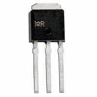
... HEXFET Power MOSFET V R DSS 100V D-Pak IRFR3410 @ 10V GS @ 10V GS - 175 300 (1.6mm from case ) Typ. ––– ––– ––– IRFR3410PbF IRFU3410PbF max I DS(on) D 31A † 39mΩ I-Pak IRFU3410 Max. Units 100 V ± 20 31† 125 ...

Page 2

Static @ T = 25°C (unless otherwise specified) J Parameter V Drain-to-Source Breakdown Voltage (BR)DSS ∆V Breakdown Voltage Temp. Coefficient /∆T (BR)DSS J R Static Drain-to-Source On-Resistance DS(on) V Gate Threshold Voltage GS(th) I Drain-to-Source Leakage Current DSS Gate-to-Source Forward ...

Page 3

PULSE WIDTH Tj = 25° Drain-to-Source Voltage (V) Fig 1. Typical Output Characteristics 1000 100 175° 25° 50V 20µs ...

Page 4

0V MHZ C iss = rss = oss = 10000 Ciss 1000 Coss 100 Crss 10 ...

Page 5

LIMITED BY PACKAGE 100 Case Temperature (°C) Fig 9. Maximum Drain Current Vs. Case Temperature 0.50 0.20 0.10 0.1 0.05 0.02 ...

Page 6

D.U 20V GS 0.01 Ω Fig 12a. Unclamped Inductive Test Circuit Fig 12b. Unclamped Inductive Waveforms Charge ...

Page 7

D.U.T + ‚ -  Driver Gate Drive P.W. D.U.T. I Waveform SD Reverse Recovery Current D.U.T. V Waveform DS Re-Applied Voltage Inductor Curent Fig 14. For N-Channel HEXFET www.irf.com + • • ƒ • - „ • ...

Page 8

EXAMPLE: THIS IS AN IRFR120 WITH ASSEMBLY LOT CODE 1234 AS SEMBLED ON WW 16, 1999 ASSEMBLY LINE "A" Note: "P" sembly line position indicates "Lead-Free" OR INTE RNATIONAL 8 INTERNATIONAL RECT IFIER IRFU120 LOGO ...

Page 9

E XAMPLE: T HIS IS AN IRFU120 WIT H ASSE MBLY LOT CODE 5678 AS SEMBLED ON WW 19, 1999 ASSE MBLY LINE "A" Note: "P" embly line pos ition indicates "Lead-Free" OR INT ...

Page 10

TR 12.1 ( .476 ) 11.9 ( .469 ) NOTES : 1. CONTROLLING DIMENSION : MILLIMETER. 2. ALL DIMENSIONS ARE SHOWN IN MILLIMETERS ( INCHES ). 3. OUTLINE CONFORMS TO EIA-481 & EIA-541. 13 INCH NOTES : 1. OUTLINE CONFORMS ...

Page 11

Note: For the most current drawings please refer to the IR website at: http://www.irf.com/package/ ...

Related keywords