NJM311M-TE3 NJR, NJM311M-TE3 Datasheet

Comparator ICs Prec Vltg Comparator

NJM311M-TE3

Manufacturer Part Number
NJM311M-TE3
Description
Comparator ICs Prec Vltg Comparator
Manufacturer
NJR
Datasheet

Specifications of NJM311M-TE3

Number Of Channels
1 Channel
Response Time
200 ns
Offset Voltage (max)
7.5 mV
Input Bias Current (max)
250 nA
Supply Voltage (max)
36 V
Supply Voltage (min)
5 V
Supply Current (max)
7.5 mA
Maximum Operating Temperature
+ 85 C
Mounting Style
SMD/SMT
Package / Case
DMP-8
Minimum Operating Temperature
- 40 C
Lead Free Status / RoHS Status
Lead free / RoHS Compliant
■ GENERAL DESCRIPTION
currents. It is also designed to operate covering a wider range
of supply voltages from Standard ±15V op amp supplies down
to the single 5V supply used for IC logic. Its output is compatible
with RTL,DTL and TTL as well as MOS circuits. Furthermore, it
can drive lamps or relays, switching voltages up to 40V at
currents as high as 50mA. Offset balancing is provided, and the
outputs can be OR wired.
■ FEATURES
■ PIN CONFIGURATION
■ EQUIVALENT CIRCUIT
Ver.2003-03-18
● Operating Voltage
● Single Supply Operation
● Single Circuit
● With V
● Response Time
● Package Outline
● Bipolar Technology
The NJM311 is a voltage comparator that has low input
IO
Trim Terminal
VOLTAGE COMPARATOR
( +5V~+36V )
( 200ns typ. )
DIP8,DMP8
NJM311D
NJM311M
PIN FUNCTION
1.
2.
3.
4.
5.
6.
7.
8.
■ PACKAGE OUTLINE
GND
+INPUT
-INPUT
V
BAL
BAL/STROBE
OUTPUT
V
-
+
NJM311D
NJM311M
- 1 -

Related parts for NJM311M-TE3

NJM311M-TE3 Summary of contents

Page 1

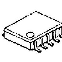
... With V Trim Terminal IO ● Response Time ● Package Outline ● Bipolar Technology ■ PIN CONFIGURATION ■ EQUIVALENT CIRCUIT Ver.2003-03-18 VOLTAGE COMPARATOR ■ PACKAGE OUTLINE ( +5V~+36V ) ( 200ns typ. ) DIP8,DMP8 PIN FUNCTION 1. GND 2. +INPUT 3. -INPUT - BAL 6. BAL/STROBE NJM311D 7. OUTPUT NJM311M + 8. V NJM311D NJM311M - 1 - ...

Page 2

ABSOLUTE MAXIMUM RATINGS PARAMETER Supply Voltage Output to Negative Supply Voltage Ground to Negative Supply Voltage Differential Input Voltage Input Voltage Power Dissipation Operating Temperature Range Storage Temperature Range ( note1 ) For supply voltage less than ±15V, the ...

Page 3

TYPICAL CHARACTERISTICS Ver.2003-03- ...

Page 4

TYPICAL CHARACTERISTICS - 4 - Ver.2003-03-18 ...

Page 5

TYPICAL APPLICATIONS Offset Null Circuit Ver.2003-03-18 Strobing [CAUTION] The specifications on this databook are only given for information , without any guarantee as regards either mistakes or omissions. The application circuits in this databook are described only to show ...

Related keywords