NE521D ON Semiconductor, NE521D Datasheet
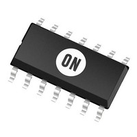
Comparator ICs Dual Diff Comparator

NE521D

Manufacturer Part Number
NE521D
Description
Comparator ICs Dual Diff Comparator
Manufacturer
ON Semiconductor
Datasheet

Specifications of NE521D

Number Of Channels
2 Channels
Output Type
Push-Pull
Response Time
9.6 ns
Offset Voltage (max)
7.5 mV
Input Bias Current (max)
20 uA
Supply Voltage (max)
7 V
Supply Current (max)
35 mA
Maximum Power Dissipation
1040 mW
Maximum Operating Temperature
+ 70 C
Mounting Style
SMD/SMT
Package / Case
SOIC-14
Minimum Operating Temperature
0 C
Lead Free Status / RoHS Status
Lead free / RoHS Compliant

Available stocks

Company
Part Number
Manufacturer
Quantity
Price
Part Number:
NE521D
Manufacturer:
NXPLIPS
Quantity:
17 306
Part Number:
NE521D
Manufacturer:
ST
0
Part Number:
NE521D
Manufacturer:
S
Quantity:
20 000
Part Number:
NE521D
Quantity:
2 390
Part Number:
NE521DG
Manufacturer:
ON
Quantity:
265
Part Number:
NE521DG
Manufacturer:
ON/安森美
Quantity:
20 000
Part Number:
NE521DR2G
Manufacturer:
ON Semiconductor
Quantity:
230
Part Number:
NE521DR2G
Manufacturer:
ON/安森美
Quantity:
20 000
NE521
High−Speed
Dual−Differential
Comparator/Sense Amp
Features
Applications
Stresses exceeding Maximum Ratings may damage the device. Maximum
Ratings are stress ratings only. Functional operation above the Recommended
Operating Conditions is not implied. Extended exposure to stresses above the
Recommended Operating Conditions may affect device reliability.
1. Derate above 25°C at the following rates:
© Semiconductor Components Industries, LLC, 2006
October, 2006 − Rev. 4
MAXIMUM RATINGS
Supply Voltage
Differential Input Voltage
Input Voltage
Maximum Power Dissipation (Note 1)
T
Thermal Resistance, Junction−to−Ambient
Operating Temperature Range
Storage Temperature Range
Operating Junction Temperature
Lead Soldering Temperature (10 sec max)
A
TTL-Compatible Strobes and Outputs
Large Common-Mode Input Voltage Range
Operates from Standard Supply Voltages
Pb−Free Packages are Available
MOS Memory Sense Amp
A-to-D Conversion
High-Speed Line Receiver
= 25°C (Still−Air)
Positive
Negative
Common Mode
Strobe/Gate
N package at 10 mW/°C
D package at 6.9 mW/°C.
Rating
N Package
D Package
N Package
D Package
Symbol
V
R
T
T
V
V+
V−
P
T
T
IDR
qJA
stg
sld
IN
A
D
J
−65 to +150
0 to 70
Value
"6.0
"5.0
+5.25
1420
1040
+230
+7.0
−7.0
100
145
150
1
°C/W
Unit
mW
°C
°C
°C
°C
V
V
V
See detailed ordering and shipping information in the package
dimensions section on page 5 of this data sheet.
1
1
STROBE 1G
OUTPUT 1Y
STROBE S
INPUT 1A
INPUT 1B
GROUND
ORDERING INFORMATION
A
WL
Y, YY = Year
WW
G
NC
CASE 751A
PIN CONNECTIONS
CASE 646
D SUFFIX
N SUFFIX
http://onsemi.com
SOIC−14
PDIP−14
1
2
3
4
5
6
7
= Assembly Location
= Wafer Lot
= Work Week
= Pb−Free Package
D, N Packages
(Top View)
Publication Order Number:
14
1
14
1
AWLYYWWG
14
13
12
11
10
DIAGRAMS
9
8
MARKING
AWLYWW
NE521N
NE521G
INPUT 2B
STROBE 2G
INPUT 2A
NC
OUTPUT 2Y
V+
V−
NE521/D

Related parts for NE521D

NE521D Summary of contents

Page 1

NE521 High−Speed Dual−Differential Comparator/Sense Amp Features • TTL-Compatible Strobes and Outputs • Large Common-Mode Input Voltage Range • Operates from Standard Supply Voltages • Pb−Free Packages are Available Applications • MOS Memory Sense Amp • A-to-D Conversion • High-Speed Line ...

Page 2

LOGIC FUNCTION TABLE + − −V < V < − ...

Page 3

DC ELECTRICAL CHARACTERISTICS Characteristic Input Offset Voltage At 25°C Overtemperature Range Input Bias Current At 25°C Overtemperature Range Input Offset Current At 25°C Overtemperature Range Common-Mode Voltage Range Input Current High Input Current Low Output Voltage High Low Supply Voltage ...

Page 4

TYPICAL PERFORMANCE CHARACTERISTICS 100mV 2 5mV 20mV 1 10mV 0 100 TIME — nS Figure 3. Response Time for ...

Page 5

... ORDERING INFORMATION Device Temperature Range NE521D NE521DG NE521DR2 NE521DR2G NE521N NE521NG †For information on tape and reel specifications, including part orientation and tape sizes, please refer to our Tape and Reel Packaging Specification Brochure, BRD8011/D. Package SOIC−14 SOIC−14 (Pb−Free) SOIC− +70° ...

Page 6

... G −T− SEATING 14 PL PLANE 0.25 (0.010 14X 0.58 *For additional information on our Pb−Free strategy and soldering details, please download the ON Semiconductor Soldering and Mounting Techniques Reference Manual, SOLDERRM/D. PACKAGE DIMENSIONS SOIC−14 CASE 751A−03 ISSUE 0.25 (0.010 ...

Page 7

... SCILLC is an Equal Opportunity/Affirmative Action Employer. This literature is subject to all applicable copyright laws and is not for resale in any manner. PUBLICATION ORDERING INFORMATION LITERATURE FULFILLMENT: Literature Distribution Center for ON Semiconductor P.O. Box 5163, Denver, Colorado 80217 USA Phone: 303−675−2175 or 800−344−3860 Toll Free USA/Canada Fax: 303− ...

Related keywords