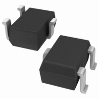
SI1304BDL-T1-E3 Vishay, SI1304BDL-T1-E3 Datasheet
Home Discrete Semiconductor Products MOSFETs, GaNFETs - Single SI1304BDL-T1-E3
Manufacturer Part Number
SI1304BDL-T1-E3
Description
MOSFET N-CH 30V 900MA SOT323-3
Specifications of SI1304BDL-T1-E3
Transistor Polarity
N-Channel
Fet Type
MOSFET N-Channel, Metal Oxide
Fet Feature
Logic Level Gate
Rds On (max) @ Id, Vgs
270 mOhm @ 900mA, 4.5V
Drain To Source Voltage (vdss)
30V
Current - Continuous Drain (id) @ 25° C
900mA
Vgs(th) (max) @ Id
1.3V @ 250µA
Gate Charge (qg) @ Vgs
2.7nC @ 4.5V
Input Capacitance (ciss) @ Vds
100pF @ 15V
Power - Max
370mW
Mounting Type
Surface Mount
Package / Case
SC-70-3, SOT-323-3
Minimum Operating Temperature
- 55 C
Configuration
Single
Drain-source Breakdown Voltage
30 V
Gate-source Breakdown Voltage
+/- 12 V
Continuous Drain Current
0.85 A
Power Dissipation
340 mW
Maximum Operating Temperature
+ 150 C
Mounting Style
SMD/SMT
Continuous Drain Current Id
900mA
Drain Source Voltage Vds
30V
On Resistance Rds(on)
385mohm
Rds(on) Test Voltage Vgs
12V
Threshold Voltage Vgs Typ
1.3V
Number Of Elements
1
Polarity
N
Channel Mode
Enhancement
Drain-source On-res
0.27Ohm
Drain-source On-volt
30V
Gate-source Voltage (max)
±12V
Drain Current (max)
850mA
Output Power (max)
Not RequiredW
Frequency (max)
Not RequiredMHz
Noise Figure
Not RequireddB
Power Gain
Not RequireddB
Drain Efficiency
Not Required%
Operating Temp Range
-55C to 150C
Operating Temperature Classification
Military
Mounting
Surface Mount
Pin Count
3
Package Type
SC-70
Lead Free Status / RoHS Status
Lead free / RoHS Compliant
Lead Free Status / RoHS Status
Lead free / RoHS Compliant, Lead free / RoHS Compliant
Other names
SI1304BDL-T1-E3TR
Available stocks
Part Number:
SI1304BDL-T1-E3
Part Number:
SI1304BDL-T1-E3
Notes:
a.
b.
c.
d.
Document Number: 73480
S–52057—Rev. B, 03–Oct–05
Drain-Source Voltage
Gate-Source Voltage
Continuous Drain Current (T
Continuous Drain Current (T
Pulsed Drain Current
Continuous Source Drain Diode Current
Continuous Source-Drain Diode Current
Maximum Power Dissipation
Maximum Power Dissipation
Operating Junction and Storage Temperature Range
Maximum Junction-to-Ambient
Maximum Junction-to-Foot (Drain)
V
Based on T
Surface mounted on 1” x 1” FR4 board.
t = 5 sec
Maximum under steady state conditions is 360 _C/W.
DS
30
30
(V)
C
Ordering Information: Si1304BDL–T1–E3
= 25_C.
0.270 @ V
0.385 @ V
G
S
r
DS(on)
1
2
J
SC-70 (3-LEADS)
= 150_C)
GS
GS
b, d
150_C)
Parameter
Parameter
(W)
= 4.5 V
= 2.5 V
Top View
N-Channel 30-V (D-S) MOSFET
I
3
D
0.90
0.75
(A)
D
a
Steady State
Q
T
T
T
T
T
T
T
T
T
T
t p 5 sec
C
C
A
A
C
A
C
C
A
A
g
New Product
= 25_C
= 70_C
= 25_C
= 70_C
= 25_C
= 25_C
= 25_C
= 70_C
= 25_C
= 70_C
1 1
1.1
(Typ)
_
Marking Code
KF
XX
Part # Code
Symbol
Symbol
T
R
R
J
V
V
I
P
P
, T
Lot Traceability
and Date Code
DM
I
I
I
I
thJA
thJF
DS
GS
D
D TrenchFETr Power MOSFET
D 100% R
S
D
stg
g
Typical
Tested
315
285
–55 to 150
0.85
0.68
0.28
0.34
0.22
Limit
"12
0.90
0.71
0.31
0.37
0.24
30
4
b, c
b, c
b, c
b, c
b, c
G
Maximum
N-Channel MOSFET
Vishay Siliconix
375
340
Si1304BDL
D
S
www.vishay.com
Unit
Unit
_C/W
_C/W
_C
W
W
RoHS
V
V
A
1
Related parts for SI1304BDL-T1-E3
SI1304BDL-T1-E3 Summary of contents
... 0.385 @ SC-70 (3-LEADS Top View Ordering Information: Si1304BDL–T1–E3 Parameter Drain-Source Voltage Gate-Source Voltage Continuous Drain Current (T Continuous Drain Current (T = 150_C) 150_C) J Pulsed Drain Current Continuous Source-Drain Diode Current Continuous Source Drain Diode Current Maximum Power Dissipation Maximum Power Dissipation ...
... Si1304BDL Vishay Siliconix _ Parameter Static Drain-Source Breakdown Voltage V Temperature Coefficient DS V Temperature Coefficient GS(th) Gate-Source Threshold Voltage Gate-Source Leakage Zero Gate Voltage Drain Current Zero Gate Voltage Drain Current a On-State Drain Current a a Drain-Source On-State Resistance Drain-Source On-State Resistance a Forward Transconductance ...
... Total Gate Charge (nC) g Document Number: 73480 S–52057—Rev. B, 03–Oct–05 New Product thru 2.0 2.5 3 1.5 2.0 Si1304BDL Vishay Siliconix Transfer Characteristics curves vs. Temp 2.0 1.5 1 –55_C A 0 25_C 125_C A 0.0 0.0 0.5 1.0 1.5 V – Gate-to-Source Voltage (V) GS Capacitance 180.0 150 ...
... Si1304BDL Vishay Siliconix Forward Diode Voltage vs. Temp 10 150_C J 1.0 0.1 0.0 0.3 0.6 V – Source-to-Drain Voltage (V) SD Threshold Voltage 1.4 1.3 1.2 = 250 1.1 1.0 0.9 0.8 0.7 0.6 –50 – – Temperature (_C) J www.vishay.com 4 New Product 25_C J 0.9 1.2 75 100 ...
... It is used to determine the current rating, when this rating falls below the package limit. Document Number: 73480 S–52057—Rev. B, 03–Oct–05 New Product _ 0.4 0.3 0.2 0.1 0.0 125 150 25 Si1304BDL Vishay Siliconix Power, De-Rating 50 75 100 125 150 Case Temperature (_C) www.vishay.com 5 ...
... Si1304BDL Vishay Siliconix Normalized Thermal Transient Impedance, Junction-to-Ambient 2 1 Duty Cycle = 0.5 0.2 0.1 0.1 0.05 0.02 Single Pulse 0.01 –4 – Normalized Thermal Transient Impedance, Junction-to-Foot 2 1 Duty Cycle = 0.5 0.2 0.1 0.1 0.05 0.02 Single Pulse 0.01 –4 –3 ...
... Vishay disclaims any and all liability arising out of the use or application of any product described herein or of any information provided herein to the maximum extent permitted by law. The product specifications do not expand or otherwise modify Vishay’ ...
Related keywords
si1303dl si1305dl si1304bdl si1303dl-t1-e3 si1302dl si1300bdl-t1-e3 si1300bdl SI1304BDL-T1-E3 datasheet SI1304BDL-T1-E3 data sheet SI1304BDL-T1-E3 pdf datasheet SI1304BDL-T1-E3 component SI1304BDL-T1-E3 part SI1304BDL-T1-E3 distributor SI1304BDL-T1-E3 RoHS SI1304BDL-T1-E3 datasheet download


