2N7002E-7-F Diodes Inc, 2N7002E-7-F Datasheet
2N7002E-7-F
Specifications of 2N7002E-7-F


Related parts for 2N7002E-7-F


2N7002E-7-F Summary of contents
Page 1
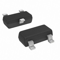
... J DS (ON) ⎯ 0.8 I D(ON ⎯ C iss ⎯ C oss ⎯ C rss ⎯ t D(ON) ⎯ t D(OFF www.diodes.com 2N7002E D S TOP VIEW Value Units 60 60 ±20 ±40 240 Value Units 300 417 °C/W -55 to +150 Typ Max Unit Test Condition ⎯ 0V 10μ ⎯ ...
Page 2
... GS 100 100 125 150 Fig. 6 Max Power Dissipation vs. Ambient Temperature www.diodes.com 2N7002E T = -55° 25° 125° GATE TO SOURCE VOLTAGE (V) GS Fig. 2 Drain Current vs. Gate-Source Voltage 10V GS 0.2 0.6 0.8 0 DRAIN CURRENT (A) D Fig Resistance vs. Drain Current ...
Page 3
... Ordering Information (Note 5) Part Number 2N7002E-7-F Notes: 5. For packaging details our website at http://www.diodes.com/datasheets/ap02007.pdf. Marking Information Date Code Key Year 2003 2004 Code P R Month Jan Feb Code 1 2 Package Outline Dimensions Suggested Pad Layout 2N7002E Document number: DS30376 Rev Case ...
Page 4
... Diodes Incorporated. Further, Customers must fully indemnify Diodes Incorporated and its representatives against any damages arising out of the use of Diodes Incorporated products in such safety-critical, life support devices or systems. Copyright © 2010, Diodes Incorporated www.diodes.com 2N7002E Document number: DS30376 Rev IMPORTANT NOTICE LIFE SUPPORT www.diodes.com 2N7002E June 2010 © Diodes Incorporated ...