NJU3430FG1-02 NJR, NJU3430FG1-02 Datasheet
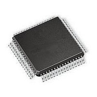
Video ICs 16 char VFD ctrlr

NJU3430FG1-02

Manufacturer Part Number
NJU3430FG1-02
Description
Video ICs 16 char VFD ctrlr
Manufacturer
NJR
Type
High Voltage Driversr
Datasheet

Specifications of NJU3430FG1-02

Package / Case
QFP-64-G1
Mounting Style
SMD/SMT
Lead Free Status / RoHS Status
Lead free / RoHS Compliant

Available stocks

Company
Part Number
Manufacturer
Quantity
Price
Part Number:
NJU3430FG1-02
Manufacturer:
POWER
Quantity:
14 660
n n GENERAL DESCRIPTION
n n FEATURES
Controller Driver for 16-character 1-line with Icon display.
tion circuit, command register, Icon display RAM, high voltage drivers,
and serial interface circuit.
interface circuits.
interface circuits.
RAM. The CG RAM stores 8 kinds of character by 5 x 7dots maxi-
mum.
mum.
operated up to 45V drive the display of 16-character 1-line with 32-
Icon.
Icon.
the LED.
the LED.
GENERAL DESCRIPTION
FEATURES
It contains character generator ROM/RAM, address counter, oscilla-
The display data or the command data is transmitted with the serial
The 16-common and 37-segment (35 for character, 2 for icon) drivers
Furthermore, the NJU3430 incorporates one Output port which drives
The NJU3430 is a Dot Matrix VFD (Vacuum Fluorescent Display)
The display data or the command data is transmitted with the serial
The character generator consists of 8,400 bits ROM and 35 x 8 bits
l l 16-character 1-line Dot Matrix VFD Controller Driver
l l Serial Interface with Microprocessor
l l Display Data RAM
l l Character Generator ROM
l l Character Generator RAM
l l Icon Display RAM
l l VFD Driving Voltage
l l Output Port for LED : 1
l l Display ON/OFF Function
l l Digit Scan Function
l l Display Duty (Contrast Control) : 8-step (8/16 to 15/16)
l l Character / Icon Shift Function
l l Display Mode (9 to 16 Digits)
l l Oscillation Circuit on-chip (External Resistor and Capacitor Required)
l l Operating Voltage
l l Package Outline
l l C-MOS Technology
16-CHARACTER 1-LINE DOT MATRIX VFD CONTROLLER DRIVER
16-character 1-line Dot Matrix VFD Controller Driver
Serial Interface with Microprocessor
Display Data RAM
Character Generator ROM
Character Generator RAM
Icon Display RAM
VFD Driving Voltage
Output Port for LED : 1
Display ON/OFF Function
Digit Scan Function
Display Duty (Contrast Control) : 8-step (8/16 to 15/16)
Character / Icon Shift Function
Display Mode (9 to 16 Digits)
Oscillation Circuit on-chip (External Resistor and Capacitor Required)
Operating Voltage
Package Outline
C-MOS Technology
Timing Signal
Timing Signal
Segment Signal
Segment Signal
: 16
: 16
: 35 (Except for Icon Segment Signal)
16 x 8 bits
16 x 8 bits
8,400 bits
8,400 bits
35 x 8 bits
35 x 8 bits
16 x 2 bits
16 x 2 bits
| V
| V
3.0V to 5.5V (Except VFD Driving Voltage)
QFP 64
QFP 64
DD
DD
-V -V
FDP
FDP
| |
: 16-character 1-line Display
: 240 Characters for 5 x 7 Dots
: 8 Patterns (5 x 7 Dots)
: Maximum 32 Icon
: Maximum 32 Icon
45V
45V
n n PACKAGE OUTLINE
PACKAGE OUTLINE
NJU3430FG1
NJU3430FG1
NJU3430
NJU3430
Jul. 2003
Ver. 3

Related parts for NJU3430FG1-02

NJU3430FG1-02 Summary of contents

Page 1

... DD DD FDP FDP : (Except for Icon Segment Signal (Except for Icon Segment Signal) 3.0V to 5.5V (Except VFD Driving Voltage) 3.0V to 5.5V (Except VFD Driving Voltage) QFP 64 QFP 64 NJU3430 NJU3430 n n PACKAGE OUTLINE PACKAGE OUTLINE NJU3430FG1 NJU3430FG1 Jul. 2003 Ver. 3 ...

Page 2

PIN CONFIGURATION PIN CONFIGURATION ...

Page 3

TERMINAL DESCRIPTION TERMINAL DESCRIPTION ...

Page 4

FUNCTION DESCRIPTION FUNCTION DESCRIPTION (1)CG RAM data and Character Dot Matrix (1)CG RAM data and Character Dot Matrix The character generator RAM (CG RAM) stores any kinds of character pattern dots written by the ...

Page 5

Table 2.CG ROM Character Pattern (ROM version -02) Table 2.CG ROM Character Pattern (ROM version -02) NJU3430 NJU3430 ...

Page 6

Function (2)Reset Function (2-1)Initialization by Reset Terminal (2-1)Initialization by Reset Terminal The NJU3430 incorporates RST terminal to initialize the all system. When the "L" level is input over 1us to the The NJU3430 incorporates RST terminal to initialize the ...

Page 7

Each instruction is shown in the Table 3. The data should be written to the RAM continuously after the RAM Each instruction is shown in the Table 3. The data should be written to the RAM continuously after ...

Page 8

Instruction (3-1)Description of each Instruction (a)Maker Testing (a)Maker Testing Set the test mode. Set the test mode. (b)Output Port Set (b)Output Port Set Set the Output Port ...

Page 9

Shift (e)Display Shift The display positions of Character and Icon are shifted by Display Shift instruction. When the codes of "LR", "M" The display positions of Character and Icon are shifted by Display ...

Page 10

Blink Set (f)Display Blink Set One blink state of Character and Icon is selected from among eight-step blink state by Display Blink Set. Non- One blink state of Character and Icon is selected ...

Page 11

Address Set (h)RAM Address Set ...

Page 12

Interface with MPU Interface with MPU The instruction and RAM data are input through the serial port. The data form is 8-bit per word, and data transfer The instruction and RAM data are input through the serial port. ...

Page 13

...

Page 14

...

Page 15

Timing Chart - Timing Chart t CSU CS t CYCE CLK t SISU PRZ t RSON RST SI Fig.3 Output Timing (CL=100pF, t Fig.3 Output Timing (CL=100pF SIH Fig.1 Data Input Timing ...

Page 16

VFD DRIVING WAVE FORM VFD DRIVING WAVE FORM OSC Oscillation Frequency ...

Page 17

APPLICATION CIRCUIT APPLICATION CIRCUIT 5x7 Dot Matrix V FD Display FDP ...

Page 18

MEMO [CAUTION] The specifications on this databook are only given for information , without any guarantee as regards either mistakes or omissions. The application circuits in this databook are described only to show representative usages of the product and not ...

Related keywords