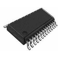
WM8196SCDS Wolfson Microelectronics, WM8196SCDS Datasheet - Page 18

WM8196SCDS
Manufacturer Part Number
WM8196SCDS
Description
Video ICs 16-Bit 12MSPS 3-Channel AFE
Manufacturer
Wolfson Microelectronics
Type
CCD/CISr
Datasheet
1.WM8196SCDS.pdf
(32 pages)
Specifications of WM8196SCDS
Operating Supply Voltage
3.3 V or 5 V
Supply Current
60 mA
Maximum Operating Temperature
+ 70 C
Package / Case
SSOP-28
Conversion Rate
12000 KSPS
Minimum Operating Temperature
- 40 C
Mounting Style
SMD/SMT
Number Of Channels
3
Resolution
16 bit
Lead Free Status / RoHS Status
Lead free / RoHS Compliant
Available stocks
Company
Part Number
Manufacturer
Quantity
Price
Company:
Part Number:
WM8196SCDS
Manufacturer:
Wolfson
Quantity:
6 000
Part Number:
WM8196SCDS
Manufacturer:
WM
Quantity:
20 000
Company:
Part Number:
WM8196SCDS/R
Manufacturer:
PANASONIC
Quantity:
66 562
Part Number:
WM8196SCDS/R
Manufacturer:
WOLFSON
Quantity:
20 000
Part Number:
WM8196SCDS/RV
Manufacturer:
WOLFSON
Quantity:
20 000
WM8196
CONTROL INTERFACE
w
Table 2 Details of Output Data Shown in Figure 15 and Figure 16.
The internal control registers are programmable via the serial digital control interface. The register
contents can be read back via the serial interface on pin OP[7]/SDO.
Note: It is recommended that a software reset is carried out after the power-up sequence, before
writing to any other register. This ensures that all registers are set to their default values (as shown
in Table 6).
SERIAL INTERFACE: REGISTER WRITE
Figure 17 shows register writing in serial mode. Three pins, SCK, SDI and SEN are used. A six-bit
address (a5, 0, a3, a2, a1, a0) is clocked in through SDI, MSB first, followed by an eight-bit data
word (b7, b6, b5, b4, b3, b2, b1, b0), also MSB first. Each bit is latched on the rising edge of SCK.
When the data has been shifted into the device, a pulse is applied to SEN to transfer the data to the
appropriate internal register. Note all valid registers have address bit a4 equal to 0 in write mode.
Figure 17 Serial Interface Register Write
A software reset is carried out by writing to Address “000100” with any value of data, i.e. Data Word
= XXXXXXXX.
SERIAL INTERFACE: REGISTER READ-BACK
Figure 18 shows register read-back in serial mode. Read-back is initiated by writing to the serial bus
as described above but with address bit a4 set to 1, followed by an 8-bit dummy data word. Writing
address (a5, 1, a3, a2, a1, a0) will cause the contents (d7, d6, d5, d4, d3, d2, d1, d0) of
corresponding register (a5, 0, a3, a2, a1, a0) to be output MSB first on pin SDO (on the falling edge
of SCK). Note that pin SDO is shared with an output pin, OP[7], therefore OEB should always be
held low when register read-back data is expected on this pin. The next word may be read in to SDI
while the previous word is still being output on SDO.
4+4+4+4-bit
multiplexed
FORMAT
OUTPUT
(nibble)
8+8-bit
SCK
SEN
SDI
a5
MUXOP[1:0]
00, 01, 10
0
11
Address
a3
a2
OUTPUT
OP[7:0]
OP[7:4]
a1
PINS
a0
b7
A = d15, d14, d13, d12, d11, d10, d9, d8
B = d7, d6, d5, d4, d3, d2, d1,d0
A = d15, d14, d13, d12
B = d11, d10, d9, d8
C = d7, d6, d5, d4
D = d3, d2, d1, d0
b6
b5
Data Word
b4
b3
OUTPUT
b2
b1
PD Rev 4.3 March 2007
b0
Production Data
18


