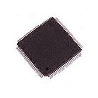
TDA8754HL17BE-S NXP Semiconductors, TDA8754HL17BE-S Datasheet - Page 28

TDA8754HL17BE-S
Manufacturer Part Number
TDA8754HL17BE-S
Description
Video ICs TRPL 8BIT VIDEO ADC
Manufacturer
NXP Semiconductors
Datasheet
1.TDA8754HL11C155.pdf
(57 pages)
Specifications of TDA8754HL17BE-S
Operating Supply Voltage
3 V to 3.6 V
Supply Current
180 mA
Maximum Operating Temperature
+ 70 C
Package / Case
SOT-486
Available Set Gain
6 dB
Bandwidth
700 MHz
Conversion Rate
170 msps
Maximum Power Dissipation
1.3 W
Minimum Operating Temperature
0 C
Mounting Style
SMD/SMT
Number Of Channels
3
Resolution
8 bit
Snr
48 dB
Lead Free Status / RoHS Status
Lead free / RoHS Compliant
Other names
TDA8754HL/17/C1,55
Philips Semiconductors
Table 29:
Table 30:
Table 31:
9397 750 14984
Product data sheet
Bit
7 to 6
5 to 3
3 to 0
Bit
7 to 4
3 to 0
Bit
Symbol
Reset
Access
Symbol
IP[1:0]
Z[2:0]
DR[2:0]
Symbol
PA[4:0]
VCO[2:0]
PLLCTRL - PLL control register (address 0Ah) bit description
PHASE - phase register (address 0Bh) bit allocation
PHASE - phase register (address 0Bh) bit description
9.8 Phase register
PA4
W
7
0
Description
charge pump current value to increase the bandwidth of the PLL
internal resistance value for the VCO filter to be selected
PLL temperature phase drift to be compensated. The optimized value of this register is 001. These
bits add a delay on the clock reference input of the PLL as a function of the temperature of the die.
Description
phase shift value for the clock pixel; see
VCO gain control; see
00 = 800 A
01 = 1200 A
10 = 1600 A
11 = 2000 A
000 = not used
001 = 1.56 k
010 = 1.25 k
011 = 1.00 k
100 = 0.80 k
101 = 0.64 k
110 = 0.51 k
111 = 0.41 k
000 = +1.75 step phase
001 = 0.3 step phase
010 = 4.3 step phase
011 = 6.2 step phase
100 = 2.2 step phase
PA3
W
6
0
Table 33
PA2
W
5
0
Rev. 06 — 16 June 2005
PA1
W
4
0
Table 32
PA0
W
3
0
Triple 8-bit video ADC up to 270 Msps
VCO2
W
2
1
© Koninklijke Philips Electronics N.V. 2005. All rights reserved.
VCO1
W
1
0
TDA8754
VCO0
W
0
1
28 of 57


