IRFD9010PBF Vishay, IRFD9010PBF Datasheet
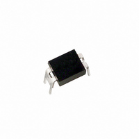
MOSFET P-CH 50V 1.1A 4-DIP

IRFD9010PBF

Manufacturer Part Number
IRFD9010PBF
Description
MOSFET P-CH 50V 1.1A 4-DIP
Manufacturer
Vishay
Series
HEXFET®r
Datasheets

Specifications of IRFD9010PBF

Transistor Polarity
P-Channel
Fet Type
MOSFET P-Channel, Metal Oxide
Fet Feature
Standard
Rds On (max) @ Id, Vgs
500 mOhm @ 580mA, 10V
Drain To Source Voltage (vdss)
50V
Current - Continuous Drain (id) @ 25° C
1.1A
Vgs(th) (max) @ Id
4V @ 250µA
Gate Charge (qg) @ Vgs
11nC @ 10V
Input Capacitance (ciss) @ Vds
240pF @ 25V
Power - Max
1W
Mounting Type
Through Hole
Package / Case
4-DIP (0.300", 7.62mm)
Minimum Operating Temperature
- 55 C
Resistance Drain-source Rds (on)
0.35 Ohms
Forward Transconductance Gfs (max / Min)
2.5 S
Drain-source Breakdown Voltage
50 V
Gate-source Breakdown Voltage
20 V
Continuous Drain Current
1.1 A
Power Dissipation
1 W
Maximum Operating Temperature
+ 125 C
Mounting Style
Through Hole
Continuous Drain Current Id
-1.1A
Drain Source Voltage Vds
-50V
On Resistance Rds(on)
350mohm
Rds(on) Test Voltage Vgs
-10V
Threshold Voltage Vgs Typ
-4V
Lead Free Status / RoHS Status
Lead free / RoHS Compliant
Lead Free Status / RoHS Status
Lead free / RoHS Compliant, Lead free / RoHS Compliant
Other names
*IRFD9010PBF
Notes
a. Repetitive rating; pulse width limited by maximum junction temperature (see fig. 11).
b. V
c. I
d. 1.6 mm from case.
* Pb containing terminations are not RoHS compliant, exemptions may apply
Document Number: 91405
S10-0998-Rev. A, 26-Apr-10
PRODUCT SUMMARY
V
R
Q
Q
Q
Configuration
ORDERING INFORMATION
Package
Lead (Pb)-free
SnPb
ABSOLUTE MAXIMUM RATINGS (T
PARAMETER
Drain-Source Voltage
Gate-Source Voltage
Continuous Drain Current
Pulsed Drain Current
Linear Derating Factor
Inductive Current, Clamped
Inductive Current, Unclamped (Avalanche Current)
Maximum Power Dissipation
Operating Junction and Storage Temperature Range
Soldering Recommendations (Peak Temperature)
DS
DS(on)
g
gs
gd
SD
DD
(Max.) (nC)
(nC)
(V)
(nC)
≤ - 4.0 A, dI/dt ≤ 75 A/μs, V
= - 25 V, starting T
D
(Ω)
HVMDIP
S
a
G
J
= 25 °C, L = 52 mH, R
V
DD
GS
≤ V
= - 10 V
DS
G
, T
P-Channel MOSFET
Single
J
- 50
≤ 175 °C.
3.8
4.1
11
g
C
= 25 Ω, I
S
D
= 25 °C, unless otherwise noted)
Power MOSFET
V
0.50
GS
L = 100 µH see fig. 14
at - 10 V
AS
= - 2.0 A (see fig. 12).
see fig. 15
T
for 10 s
C
= 25 °C
T
T
C
HVMDIP
IRFD9010PbF
SiHFD9010-E3
IRFD9010
SiHFD9010
C
= 100 °C
FEATURES
• For Automatic Insertion
• Compact, End Stackable
• Fast Switching
• Low Drive Current
• Easy Paralleled
• Excellent Temperature Stability
• P-Channel Versatility
• Compliant to RoHS Directive 2002/95/EC
DESCRIPTION
The HVMDIP technology is the key to Vishay’s advanced
line of power MOSFET transistors. The efficient geometry
and unique processing of the HVMDIP design achieves
very
transconductance and extreme device ruggedness.
The p-channel HVMDIPs are designed for application which
require the convenience of reverse polarity operation. They
retain all of the features of the more common n-channel
HVMDIPs such as voltage control, very fast switching, ease
of paralleling, and excellent temperature stability.
P-channels HVMDIPs are intended for use in power stages
where complementary symmetry with n-channel devices
offers circuit simplification. They are also very useful in drive
stages because of the circuit versatility offered by the
reverse polarity connection. Applications include motor
control, audio amplifiers, switched mode converters, control
circuits and pulse amplifiers.
= 25 °C
low
SYMBOL
T
on-state
J
V
V
I
I
P
, T
DM
LM
I
I
DS
GS
D
L
D
stg
IRFD9010, SiHFD9010
resistance
- 55 to + 150
LIMIT
- 0.68
300
± 20
- 1.1
- 8.8
0.01
- 8.8
- 1.5
- 50
1
Vishay Siliconix
d
combined
www.vishay.com
with
UNIT
W/°C
°C
W
V
A
A
high
1

Related parts for IRFD9010PBF

IRFD9010PBF Summary of contents

Page 1

... They are also very useful in drive P-Channel MOSFET stages because of the circuit versatility offered by the reverse polarity connection. Applications include motor control, audio amplifiers, switched mode converters, control circuits and pulse amplifiers. HVMDIP IRFD9010PbF SiHFD9010-E3 IRFD9010 SiHFD9010 = 25 °C, unless otherwise noted ° ...

Page 2

... IRFD9010, SiHFD9010 Vishay Siliconix THERMAL RESISTANCE RATINGS PARAMETER Maximum Junction-to-Ambient SPECIFICATIONS ( °C, unless otherwise noted) J PARAMETER Static Drain-Source Breakdown Voltage V Temperature Coefficient DS Gate-Source Threshold Voltage Gate-Source Leakage Zero Gate Voltage Drain Current On-State Drain Current Drain-Source On-State Resistance Forward Transconductance Dynamic ...

Page 3

... Fig Normalized On-Resistance vs. Temperature 500 - 10 V 400 - 8 V 300 - 7 V 200 100 - Fig Typical Capacitance vs. Drain-to-Source Voltage Fig Typical Gate Charge vs. Gate-to-Source Voltage IRFD9010, SiHFD9010 Vishay Siliconix 4 100 120 140 T , Junction Temperature (° MHz Shorted iss rss oss ds ...

Page 4

... IRFD9010, SiHFD9010 Vishay Siliconix 100 T = 150 ° ° 0 Source-to-Drain Voltage (V) SD Fig Typical Source-Drain Diode Forward Voltage 100 Operation in this Area Limited by R DS(on 0 ° 150 °C J Single Pulse 0. Drain-to-Source Voltage (V) DS Fig Maximum Safe Operating Area www.vishay.com 4 2.0 1.6 1.2 ...

Page 5

... D.U 0. Fig. 12a - Unclamped Inductive Test Circuit Fig. 12b - Unclamped Inductive Waveforms Document Number: 91405 S10-0998-Rev. A, 26-Apr-10 0.001 0.01 0 Rectangular Pulse Duration ( IRFD9010, SiHFD9010 Vishay Siliconix Notes: 1. Duty Factor Peak thJC 100 Charge Fig. 13a - Basic Gate Charge Waveform Current regulator Same type as D.U.T. 50 kΩ ...

Page 6

... V GS Vishay Siliconix maintains worldwide manufacturing capability. Products may be manufactured at one of several qualified locations. Reliability data for Silicon Technology and Package Reliability represent a composite of all qualified locations. For related documents such as package/tape drawings, part marking, and reliability data, see www.vishay.com/ppg?91405. www.vishay.com ...

Page 7

... Vishay product could result in personal injury or death. Customers using or selling Vishay products not expressly indicated for use in such applications their own risk and agree to fully indemnify and hold Vishay and its distributors harmless from and against any and all claims, liabilities, expenses and damages arising or resulting in connection with such use or sale, including attorneys fees, even if such claim alleges that Vishay or its distributor was negligent regarding the design or manufacture of the part ...

Related keywords