IRLI620G Vishay, IRLI620G Datasheet

MOSFET N-CH 200V 4A TO220FP

IRLI620G

Manufacturer Part Number
IRLI620G
Description
MOSFET N-CH 200V 4A TO220FP
Manufacturer
Vishay
Series
HEXFET®r
Datasheets

Specifications of IRLI620G

Fet Type
MOSFET N-Channel, Metal Oxide
Fet Feature
Logic Level Gate
Rds On (max) @ Id, Vgs
800 mOhm @ 2.4A, 5V
Drain To Source Voltage (vdss)
200V
Current - Continuous Drain (id) @ 25° C
4A
Vgs(th) (max) @ Id
2V @ 250µA
Gate Charge (qg) @ Vgs
16nC @ 10V
Input Capacitance (ciss) @ Vds
360pF @ 25V
Power - Max
30W
Mounting Type
Through Hole
Package / Case
TO-220-3 Full Pack (Straight Leads, Isolated), ITO-220AB
Transistor Polarity
N Channel
Continuous Drain Current Id
4A
Drain Source Voltage Vds
200V
On Resistance Rds(on)
800mohm
Rds(on) Test Voltage Vgs
5V
Threshold Voltage Vgs Typ
2V
Configuration
Single
Resistance Drain-source Rds (on)
0.8 Ohms
Drain-source Breakdown Voltage
200 V
Gate-source Breakdown Voltage
+/- 10 V
Continuous Drain Current
4 A
Power Dissipation
30 W
Maximum Operating Temperature
+ 150 C
Mounting Style
Through Hole
Minimum Operating Temperature
- 55 C
Lead Free Status / RoHS Status
Contains lead / RoHS non-compliant
Lead Free Status / RoHS Status
Contains lead / RoHS non-compliant, Contains lead / RoHS non-compliant
Other names
*IRLI620G

Available stocks

Company
Part Number
Manufacturer
Quantity
Price
Part Number:
IRLI620G
Manufacturer:
IR
Quantity:
12 500
Company:
Part Number:
IRLI620GPBF
Quantity:
70 000
Thermal Resistance
Third Generation HEXFETs from International Rectifier provide the designer
with the best combination of fast switching, ruggedized device design, low on-
resistance and cost-effectiveness.
The TO-220 Fullpak eliminates the need for additional insulating hardware in
commercial-industrial applications. The moulding compound used provides a
high isolation capability and a low thermal resistance between the tab and external
heatsink. This isolation is equivalent to using a 100 micron mica barrier with
standard TO-220 product. The Fullpak is mounted to a heatsink using a single clip
or by a single screw fixing.
HEXFET
Description
Absolute Maximum Ratings
I
I
I
P
V
E
I
E
dv/dt
T
T
R
R
D
D
DM
AR
J
D
GS
AS
AR
STG
@ T
@ T
Isolated Package
High Voltage Isolation = 2.5KVRMS
Sink to Lead Creepage Dist. 4.8mm
Logic-Level Gate Drive
R
Fast Switching
Ease of paralleling
JC
JA
@T
DS(ON)
C
C
C
= 25°C
= 100°C
= 25°C
®
Specified at V
Power MOSFET
Continuous Drain Current, V
Pulsed Drain Current
Power Dissipation
Linear Derating Factor
Gate-to-Source Voltage
Single Pulse Avalanche Energy
Avalanche Current
Repetitive Avalanche Energy
Peak Diode Recovery dv/dt
Operating Junction and
Storage Temperature Range
Soldering Temperature, for 10 seconds
Mounting torque, 6-32 or M3 screw.
Junction-to-Case
Junction-to-Ambient
GS
Parameter
Parameter
= 4V & 5V
GS
GS
@ 5.0V
@ 5.0V
Min.
––––
––––
300 (1.6mm from case)
10 lbf•in (1.1N•m)
-55 to + 150
Max.
0.24
±10
4.0
2.6
4.0
3.0
5.0
16
30
62
Typ.
––––
––––
IRLI620G
V
R
I
D
DSS
DS(on)
= 4.0A
= 200V
PD - 9.1235
Max.
4.1
= 0.80
65
Revision 0
Units
Units
°C/W
W/°C
V/ns
mJ
mJ
°C
W
A
V
A

Related parts for IRLI620G

IRLI620G Summary of contents

Page 1

... Min. Typ. –––– –––– –––– –––– 9.1235 IRLI620G V = 200V DSS R = 0.80 DS(on 4.0A D Units A W W/°C V ...

Page 2

... IRLI620G Electrical Characteristics @ T Parameter V Drain-to-Source Breakdown Voltage (BR)DSS Breakdown Voltage Temp. Coefficient (BR)DSS J R Static Drain-to-Source On-Resistance DS(ON) V Gate Threshold Voltage GS(th) g Forward Transconductance fs I Drain-to-Source Leakage Current DSS Gate-to-Source Forward Leakage I GSS Gate-to-Source Reverse Leakage Q Total Gate Charge g Q Gate-to-Source Charge ...

Page 3

... A 0.1 0.1 10 100 V Fig 2. Typical Output Characteristics, 2 5.2A D 2.0 1.5 1.0 0.5 A 0.0 4.5 5.0 -60 - Junction Temperature (°C) Fig 4. Normalized On-Resistance IRLI620G VGS 7.50V 5.00V 4.00V 3.50V 3.00V 2.75V 2.50V 2.25V 20µs PULSE WIDTH T = 150° Drain-to-Source Voltage ( 150 5.0V ...

Page 4

... IRLI620G 2000 1MHz iss rss oss ds gd 1500 C iss C oss 1000 C 500 rss Drain-to-Source Voltage (V) DS Fig 5. Typical Capacitance Vs. Drain-to-Source Voltage 100 150° 25° 0.1 0.3 0.6 0 Source-to-Drain Voltage (V) SD Fig 7. Typical Source-Drain Diode Forward Voltage SHORTED 100 0 Fig 6. Typical Gate Charge Vs. ...

Page 5

... Fig 9. Maximum Drain Current Vs. Case Temperature 0 0.01 0.00001 0.0001 Fig 11. Maximum Effective Transient Thermal Impedance, Junction-to-Case Pulse Width Duty Factor Fig 10a. Switching Time Test Circuit A 125 150 Fig 10b. Switching Time Waveforms 0.001 0. Rectangular Pulse Duration (sec) 1 IRLI620G D.U. 5.0 V µ 0 ...

Page 6

... IRLI620G 5.0V Fig 12a. Unclamped Inductive Test Circuit Fig 12b. Unclamped Inductive Waveforms 5.0V Fig 13a. Basic Gate Charge Waveform 150 TOP 125 BOTTOM 4.0A 100 50V 100 Starting T , Juntion Temperature (°C) J Fig 12c. Maximum Avalanche Energy Vs. Drain Current Fig 13b. Gate Charge Test Circuit ...

Page 7

... Peak Diode Recovery dv/dt Test Circuit Circuit Layout Considerations D.U.T Low Stray Inductance Ground Plane Low Leakage Inductance Current Transformer R dv/dt controlled Driver same type as D.U.T. I controlled by Duty Factor "D" SD D.U.T. - Device Under Test * VGS = 5V for Logic Level Devices Fig 14. For N-Channel HEXFETS IRLI620G ...
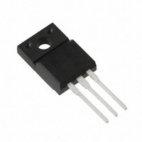
Page 8

... IRLI620G Package Outline TO-220 Full-Pak Part Marking Information TO-220 Full-Pak WORLD HEADQUARTERS: 233 Kansas St., El Segundo, California 90245, Tel: (310) 322 3331 EUROPEAN HEADQUARTERS: Hurst Green, Oxted, Surrey RH8 9BB, UK Tel: (44) 0883 713215 IR CANADA: 7321 Victoria Park Ave., Suite 201, Markham, Ontario L3R 3L1, Tel: (905) 475 1897 IR GERMANY: Saalburgstrasse 157, 61350 Bad Homburg Tel: 6172 37066 IR ITALY: Via Liguria 49, 10071 Borgaro, Torino Tel: (39) 1145 10111 IR FAR EAST: K& ...

Related keywords