IRFP32N50KPBF Vishay, IRFP32N50KPBF Datasheet - Page 2
IRFP32N50KPBF
Manufacturer Part Number
IRFP32N50KPBF
Description
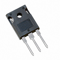
MOSFET N-CH 500V 32A TO-247AC
Manufacturer
Vishay
Type
Power MOSFETr
Specifications of IRFP32N50KPBF
Transistor Polarity
N-Channel
Fet Type
MOSFET N-Channel, Metal Oxide
Fet Feature
Standard
Rds On (max) @ Id, Vgs
160 mOhm @ 32A, 10V
Drain To Source Voltage (vdss)
500V
Current - Continuous Drain (id) @ 25° C
32A
Vgs(th) (max) @ Id
5V @ 250µA
Gate Charge (qg) @ Vgs
190nC @ 10V
Input Capacitance (ciss) @ Vds
5280pF @ 25V
Power - Max
460W
Mounting Type
Through Hole
Package / Case
TO-247-3 (Straight Leads), TO-247AC
Minimum Operating Temperature
- 55 C
Configuration
Single
Resistance Drain-source Rds (on)
0.16 Ohm @ 10 V
Drain-source Breakdown Voltage
500 V
Gate-source Breakdown Voltage
+/- 30 V
Continuous Drain Current
32 A
Power Dissipation
460000 mW
Maximum Operating Temperature
+ 150 C
Mounting Style
Through Hole
Continuous Drain Current Id
32A
Drain Source Voltage Vds
500V
On Resistance Rds(on)
160mohm
Rds(on) Test Voltage Vgs
10V
Threshold Voltage Vgs Typ
5V
Number Of Elements
1
Polarity
N
Channel Mode
Enhancement
Drain-source On-res
0.16Ohm
Drain-source On-volt
500V
Gate-source Voltage (max)
±30V
Drain Current (max)
32A
Output Power (max)
Not RequiredW
Frequency (max)
Not RequiredMHz
Noise Figure
Not RequireddB
Power Gain
Not RequireddB
Drain Efficiency
Not Required%
Operating Temp Range
-55C to 150C
Operating Temperature Classification
Military
Mounting
Through Hole
Pin Count
3 +Tab
Package Type
TO-247AC
Lead Free Status / RoHS Status
Lead free / RoHS Compliant
Lead Free Status / RoHS Status
Lead free / RoHS Compliant, Lead free / RoHS Compliant
Other names
*IRFP32N50KPBF
Available stocks
Company
Part Number
Manufacturer
Quantity
Price

Part Number:
IRFP32N50KPBF
Manufacturer:
IR
Quantity:
20 000


Diode Characteristics
Static @ T
Dynamic @ T
Document Number: 91221
‚
ƒ
Notes:
I
I
Symbol
V
∆V
R
V
g
Q
Q
Q
t
t
t
t
C
C
C
C
C
C
Symbol
I
I
V
t
Q
I
t
DSS
GSS
d(on)
d(off)
SM
r
f
S
rr
RRM
on
fs
(BR)DSS
GS(th)
DS(on)
iss
oss
rss
oss
oss
oss
SD
g
gs
gd
rr
Repetitive rating; pulse width limited by
I
(BR)DSS
T
max. junction temperature.
Starting T
SD
I
AS
J
eff.
≤ 150°C
≤ 32A, di/dt ≤ 197A/µs, V
= 32A,
/∆T
J
J
Drain-to-Source Leakage Current
Drain-to-Source Breakdown Voltage
Breakdown Voltage Temp. Coefficient
Static Drain-to-Source On-Resistance
Gate Threshold Voltage
Gate-to-Source Forward Leakage
Gate-to-Source Reverse Leakage
Forward Transconductance
Total Gate Charge
Gate-to-Source Charge
Gate-to-Drain ("Miller") Charge
Turn-On Delay Time
Rise Time
Turn-Off Delay Time
Fall Time
Input Capacitance
Output Capacitance
Reverse Transfer Capacitance
Output Capacitance
Output Capacitance
Effective Output Capacitance
Continuous Source Current
(Body Diode)
Pulsed Source Current
(Body Diode)
Diode Forward Voltage
Reverse Recovery Time
Reverse RecoveryCharge
Reverse RecoveryCurrent
Forward Turn-On Time
= 25°C, L = 0.87mH, R
J
= 25°C (unless otherwise specified)
J
= 25°C (unless otherwise specified)
Parameter
Parameter
Parameter
DD
≤ V
G
(BR)DSS
= 25Ω,
,
„
…
Pulse width ≤ 400µs; duty cycle ≤ 2%.
C
as C
500
–––
––– 0.135 0.16
–––
–––
–––
–––
–––
–––
–––
–––
–––
–––
–––
–––
–––
–––
–––
–––
–––
Min. Typ. Max. Units
3.0
Min. Typ. Max. Units
Min. Typ. Max. Units
14
–––
–––
–––
–––
–––
–––
oss
Intrinsic turn-on time is negligible (turn-on is dominated by L
eff. is a fixed capacitance that gives the same charging time
oss
5280 –––
5630 –––
0.54 –––
–––
–––
–––
–––
–––
––– -100
–––
–––
–––
–––
120
550
155
265
–––
–––
–––
530
while V
9.0
28
48
54
45
30
–––
250
100
13.5
–––
190
–––
–––
–––
–––
–––
–––
–––
–––
130
800
–––
5.0
1.5
50
59
84
32
DS
is rising from 0 to 80% V
V/°C
µA
µA
nA
nC
ns
µC
pF
ns
V
Ω
V
S
A
V
A
V
Reference to 25°C, I
V
V
V
V
V
V
V
V
V
V
I
R
V
V
V
ƒ = 1.0MHz, See Fig. 5
V
V
V
MOSFET symbol
showing the
integral reverse
p-n junction diode.
T
T
di/dt = 100A/µs „
I
D
D
GS
GS
DS
DS
DS
GS
GS
DS
DS
GS
DD
GS
GS
DS
GS
GS
GS
J
J
G
= 32A
= 32A
= 25°C, I
= 25°C, I
= 4.3Ω
= V
= 500V, V
= 400V, V
= 0V, I
= 10V, I
= 30V
= -30V
= 50V, I
= 400V
= 10V „
= 250V
= 10V „
= 0V
= 25V
= 0V, V
= 0V, V
= 0V, V
GS
, I
D
S
F
D
DS
D
D
DS
DS
Conditions
= 250µA
Conditions
Conditions
= 32A, V
= 32A
= 250µA
= 32A
= 32A
GS
GS
DSS
= 0V to 400V …
= 1.0V, ƒ = 1.0MHz
= 400V, ƒ = 1.0MHz
= 0V
= 0V, T
.
D
www.vishay.com
= 1mA†
GS
„
J
= 0V „
G
= 150°C
S
+L
D
S
D
)
2
Related parts for IRFP32N50KPBF
Image
Part Number
Description
Manufacturer
Datasheet
Request
R

Part Number:
Description:
357-036-542-201 CARDEDGE 36POS DL .156 BLK LOPRO
Manufacturer:
Vishay
Datasheet:
Part Number:
Description:
357-036-542-201 CARDEDGE 36POS DL .156 BLK LOPRO
Manufacturer:
Vishay
Datasheet:
Part Number:
Description:
357-036-542-201 CARDEDGE 36POS DL .156 BLK LOPRO
Manufacturer:
Vishay
Datasheet:
Part Number:
Description:
357-036-542-201 CARDEDGE 36POS DL .156 BLK LOPRO
Manufacturer:
Vishay
Datasheet:
Part Number:
Description:
357-036-542-201 CARDEDGE 36POS DL .156 BLK LOPRO
Manufacturer:
Vishay
Datasheet:
Part Number:
Description:
357-036-542-201 CARDEDGE 36POS DL .156 BLK LOPRO
Manufacturer:
Vishay
Datasheet:
Part Number:
Description:
357-036-542-201 CARDEDGE 36POS DL .156 BLK LOPRO
Manufacturer:
Vishay
Datasheet:
Part Number:
Description:
357-036-542-201 CARDEDGE 36POS DL .156 BLK LOPRO
Manufacturer:
Vishay
Datasheet:
Part Number:
Description:
357-036-542-201 CARDEDGE 36POS DL .156 BLK LOPRO
Manufacturer:
Vishay
Datasheet:
Part Number:
Description:
357-036-542-201 CARDEDGE 36POS DL .156 BLK LOPRO
Manufacturer:
Vishay
Datasheet:
Part Number:
Description:
357-036-542-201 CARDEDGE 36POS DL .156 BLK LOPRO
Manufacturer:
Vishay
Datasheet:
Part Number:
Description:
357-036-542-201 CARDEDGE 36POS DL .156 BLK LOPRO
Manufacturer:
Vishay
Datasheet:
Part Number:
Description:
357-036-542-201 CARDEDGE 36POS DL .156 BLK LOPRO
Manufacturer:
Vishay
Datasheet:
Part Number:
Description:
357-036-542-201 CARDEDGE 36POS DL .156 BLK LOPRO
Manufacturer:
Vishay
Datasheet:
Part Number:
Description:
357-036-542-201 CARDEDGE 36POS DL .156 BLK LOPRO
Manufacturer:
Vishay
Datasheet: