IRF7811AVPBF International Rectifier, IRF7811AVPBF Datasheet
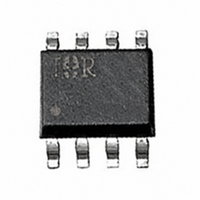
MOSFET N-CH 30V 10.8A 8-SOIC

IRF7811AVPBF

Manufacturer Part Number
IRF7811AVPBF
Description
MOSFET N-CH 30V 10.8A 8-SOIC
Manufacturer
International Rectifier
Series
HEXFET®r
Datasheets

Specifications of IRF7811AVPBF

Fet Type
MOSFET N-Channel, Metal Oxide
Fet Feature
Logic Level Gate
Rds On (max) @ Id, Vgs
14 mOhm @ 15A, 4.5V
Drain To Source Voltage (vdss)
30V
Current - Continuous Drain (id) @ 25° C
10.8A
Vgs(th) (max) @ Id
3V @ 250µA
Gate Charge (qg) @ Vgs
26nC @ 5V
Input Capacitance (ciss) @ Vds
1801pF @ 10V
Power - Max
2.5W
Mounting Type
Surface Mount
Package / Case
8-SOIC (3.9mm Width)
Current, Drain
10.8 A
Gate Charge, Total
17 nC
Package Type
SO-8
Polarization
N-Channel
Power Dissipation
2.5 W
Resistance, Drain To Source On
11 Milliohms
Temperature, Operating, Maximum
+150 °C
Temperature, Operating, Minimum
-55 °C
Time, Turn-off Delay
43 ns
Time, Turn-on Delay
8.6 ns
Voltage, Breakdown, Drain To Source
30 V
Voltage, Forward, Diode
1.3 V
Voltage, Gate To Source
±20 V
Lead Free Status / RoHS Status
Lead free / RoHS Compliant

Available stocks

Company
Part Number
Manufacturer
Quantity
Price
Part Number:
IRF7811AVPBF
Manufacturer:
IR
Quantity:
20 000
• N-Channel Application-Specific MOSFETs
• Ideal for CPU Core DC-DC Converters
• Low Conduction Losses
• Low Switching Losses
• Minimizes Parallel MOSFETs for high current
• 100% R
• Lead-Free
Description
This new device employs advanced HEXFET Power
MOSFET technology to achieve an unprecedented
balance of on-resistance and gate charge. The reduced
conduction and switching losses make it ideal for high
efficiency DC-DC converters that power the latest
generation of microprocessors.
The IRF7811AV has been optimized for all parameters
that are critical in synchronous buck converters including
R
The IRF7811AV offers an extremely low combination of
Q
synchronous FET applications.
The package is designed for vapor phase, infra-red,
convection, or wave soldering techniques. Power
dissipation of greater than 2W is possible in a typical
PCB mount application.
www.irf.com
Drain-to-Source Voltage
Gate-to-Source Voltage
Continuous Output Current
(V
Pulsed Drain Current
Power Dissipation
Junction & Storage Temperature Range
Continuous Source Current (Body Diode)
Pulsed Source Current
Maximum Junction-to-Ambient
Maximum Junction-to-Lead
Absolute Maximum Ratings
Thermal Resistance
DS(on)
sw
applications
GS
& R
≥ 4.5V)
, gate charge and Cdv/dt-induced turn-on immunity.
DS(on)
G
Tested
for reduced losses in both control and
Parameter
ÃÃÃÃÃÃÃÃÃÃ
Parameter
h
T
T
T
T
A
A
L
L
= 25°C
= 90°C
= 25°C
= 90°C
Symbol
T
Symbol
J
R
R
V
V
I
, T
P
I
DM
I
I
SM
θJA
θJL
DS
GS
D
S
D
STG
DEVICE CHARACTERISTICS…
SO-8
R
Q
Q
DS(on)
IRF7811AVPbF
IRF7811AVPbF
Q
Typ
–––
–––
OSS
SW
G
IRF7811AV
-55 to 150
10.8
11.8
±20
100
2.5
3.0
2.5
30
50
G
S
S
S
IRF7811AV
11 mΩ
6.7 nC
8.1 nC
17 nC
Max
50
20
1
2
3
4
Top View
PD-95265
8
7
6
5
Units
Units
°C/W
°C
W
V
A
A
D
D
D
D
A
A
08/17/04
1

Related parts for IRF7811AVPBF

IRF7811AVPBF Summary of contents

Page 1

... Power Dissipation Junction & Storage Temperature Range Continuous Source Current (Body Diode) ™ Pulsed Source Current Thermal Resistance Parameter h Maximum Junction-to-Ambient hà Maximum Junction-to-Lead www.irf.com IRF7811AVPbF IRF7811AVPbF SO-8 DEVICE CHARACTERISTICS… R DS(on OSS Symbol ...

Page 2

... IRF7811AVPbF Electrical Characteristics Parameter Drain-to-Source Breakdown Voltage Static Drain-to-Source On-Resistance Gate Threshold Voltage Drain-to-Source Leakage Current Gate-to-Source Leakage Current Total Gate Charge, Control FET Total Gate Charge, Synch FET Pre-Vth Gate-to-Source Charge Post-Vth Gate-to-Source Charge Gate-to-Drain ("Miller") Charge Switch Charge ( gs2 ...

Page 3

... Figure 4. Typical Capacitance vs. Drain-to-Source Voltage 100 10 ° 15V DS 0.1 4.0 4.5 5.0 0.3 Figure 6. Typical Source-Drain Diode Forward Voltage IRF7811AVPbF 15A Total Gate Charge (nC 0V MHZ C iss = SHORTED C rss = oss = Ciss Coss Crss Drain-to-Source Voltage (V) ° 150 C J ° ...

Page 4

... IRF7811AVPbF 100 D = 0.50 0.20 10 0.10 0.05 0.02 1 0.01 SINGLE PULSE (THERMAL RESPONSE) 0.1 0.0001 0.001 Figure 7. Maximum Effective Transient Thermal Impedance, Junction-to-Ambient 125nS V ds 90% 10 d(on) 4 0.01 0 Rectangular Pulse Duration (sec Schottky -6A 450 50 u Repetition rate:100Hz Mic4452BM 450 50 Ohms probe f(v) ...

Page 5

... L 7 6.46 [.255] 3X 1.27 [.050] DAT E CODE (YWW DES IGNAT ES LEAD-FREE PRODUCT (OPT IONAL LAS T DIGIT YEAR WW = WEEK XXXX EMBLY CODE F7101 LOT CODE PART NUMBER IRF7811AVPbF INCHES MILLIMETERS DIM MIN MAX MIN MAX A .0532 .0688 1.35 1.75 A1 .0040 .0098 ...

Page 6

... IRF7811AVPbF SO-8 Tape and Reel 8.1 ( .318 ) 7.9 ( .312 ) NOTES: 1. CONTROLLING DIMENSION : MILLIMETER. 2. ALL DIMENSIONS ARE SHOWN IN MILLIMETERS(INCHES). 3. OUTLINE CONFORMS TO EIA-481 & EIA-541. NOTES : 1. CONTROLLING DIMENSION : MILLIMETER. 2. OUTLINE CONFORMS TO EIA-481 & EIA-541. IR WORLD HEADQUARTERS: 233 Kansas St., El Segundo, California 90245, USA Tel: (310) 252-7105 ...

Related keywords