IRF6216PBF International Rectifier, IRF6216PBF Datasheet
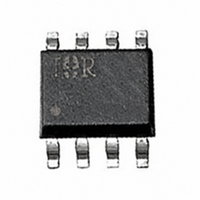
MOSFET P-CH 150V 2.2A 8-SOIC

IRF6216PBF

Manufacturer Part Number
IRF6216PBF
Description
MOSFET P-CH 150V 2.2A 8-SOIC
Manufacturer
International Rectifier
Series
HEXFET®r
Type
Power MOSFETr
Datasheets

Specifications of IRF6216PBF

Fet Type
MOSFET P-Channel, Metal Oxide
Fet Feature
Standard
Rds On (max) @ Id, Vgs
240 mOhm @ 1.3A, 10V
Drain To Source Voltage (vdss)
150V
Current - Continuous Drain (id) @ 25° C
2.2A
Vgs(th) (max) @ Id
5V @ 250µA
Gate Charge (qg) @ Vgs
49nC @ 10V
Input Capacitance (ciss) @ Vds
1280pF @ 25V
Power - Max
2.5W
Mounting Type
Surface Mount
Package / Case
8-SOIC (3.9mm Width)
Channel Type
P
Current, Drain
-2.2 A
Gate Charge, Total
33 nC
Package Type
SO-8
Polarization
P-Channel
Power Dissipation
2.5 W
Resistance, Drain To Source On
0.24 Ohm
Temperature, Operating, Maximum
+150 °C
Temperature, Operating, Minimum
-55 °C
Time, Turn-off Delay
33 ns
Time, Turn-on Delay
18 ns
Transconductance, Forward
2.7 S
Voltage, Breakdown, Drain To Source
-150 V
Voltage, Drain To Source
-150 V
Voltage, Forward, Diode
-1.6 V
Voltage, Gate To Source
±20 V
Number Of Elements
1
Polarity
P
Channel Mode
Enhancement
Drain-source On-res
0.24Ohm
Drain-source On-volt
150V
Gate-source Voltage (max)
±20V
Continuous Drain Current
2.2A
Operating Temp Range
-55C to 150C
Operating Temperature Classification
Military
Mounting
Surface Mount
Pin Count
8
Configuration
Single Quad Drain Triple Source
Transistor Polarity
P-Channel
Resistance Drain-source Rds (on)
240 m Ohms
Drain-source Breakdown Voltage
- 150 V
Gate-source Breakdown Voltage
20 V
Maximum Operating Temperature
+ 150 C
Mounting Style
SMD/SMT
Fall Time
26 ns
Gate Charge Qg
33 nC
Minimum Operating Temperature
- 55 C
Rise Time
15 ns
Lead Free Status / RoHS Status
Lead free / RoHS Compliant

Available stocks

Company
Part Number
Manufacturer
Quantity
Price
Part Number:
IRF6216PBF
Manufacturer:
ST
Quantity:
10
Thermal Resistance
l
l
l
l
l
Absolute Maximum Ratings
www.irf.com
Applications
I
I
I
P
V
dv/dt
T
T
Notes  through
Benefits
Symbol
R
R
D
D
DM
J
STG
D
GS
θJL
θJA
@ T
@ T
Effective C
App. Note AN1001)
and Current
@T
Reset Switch for Active Clamp Reset
DC-DC converters
Lead-Free
Low Gate to Drain Charge to Reduce
Fully Characterized Capacitance Including
Fully Characterized Avalanche Voltage
Switching Losses
A
A
A
= 25°C
= 70°C
= 25°C
OSS
Continuous Drain Current, V
Pulsed Drain Current 
Power Dissipation„
Linear Derating Factor
Gate-to-Source Voltage
Peak Diode Recovery dv/dt
Operating Junction and
Storage Temperature Range
Soldering Temperature, for 10 seconds
Junction-to-Drain Lead
Junction-to-Ambient
to Simplify Design (See
are on page 8
Parameter
Parameter
SMPS MOSFET
GS
GS
@ 10V
@ 10V
G
S
S
S
V
-150V
DSS
1
2
3
4
Top View
IRF6216PbF
Typ.
300 (1.6mm from case )
–––
–––
0.240
HEXFET
-55 to + 150
8
6
5
7
R
Max.
0.02
-2.2
-1.9
± 20
DS(on)
-19
2.5
7.8
W
D
D
D
D
A
@V
®
GS
Power MOSFET
max
Max.
20
50
=-10V -2.2A
SO-8
Units
Units
W/°C
°C/W
I
V/ns
D
°C
W
A
V
1
06/06/05

Related parts for IRF6216PBF

IRF6216PBF Summary of contents

Page 1

... J T Storage Temperature Range STG Soldering Temperature, for 10 seconds Thermal Resistance Symbol Parameter R Junction-to-Drain Lead θJL R Junction-to-Ambient θJA Notes  through „ are on page 8 www.irf.com SMPS MOSFET IRF6216PbF V DSS -150V Top View @ 10V GS @ 10V GS 300 (1.6mm from case ) Typ. ––– ...

Page 2

... IRF6216PbF Static @ T = 25°C (unless otherwise specified) J Parameter V Drain-to-Source Breakdown Voltage (BR)DSS ∆V Breakdown Voltage Temp. Coefficient /∆T (BR)DSS J R Static Drain-to-Source On-Resistance DS(on) V Gate Threshold Voltage GS(th) I Drain-to-Source Leakage Current DSS Gate-to-Source Forward Leakage I GSS Gate-to-Source Reverse Leakage Dynamic @ T = 25°C (unless otherwise specified) ...

Page 3

... Fig 2. Typical Output Characteristics 2 2.0 ° 150 C J 1.5 1.0 0.5 0.0 -60 -40 7.5 8.0 Fig 4. Normalized On-Resistance IRF6216PbF VGS -15V -12V -10V -8.0V -7.0V -6.0V -5.5V -5.0V -5.0V 20µs PULSE WIDTH ° 150 Drain-to-Source Voltage (V) DS -2.2A ...

Page 4

... IRF6216PbF 10000 0V, C iss = rss = oss = Ciss 1000 Coss 100 Crss Drain-to-Source Voltage (V) Fig 5. Typical Capacitance Vs. Drain-to-Source Voltage 100 10 ° 150 0.1 0.4 0.6 0.8 -V ,Source-to-Drain Voltage (V) SD Fig 7. Typical Source-Drain Diode Forward Voltage MHZ SHORTED 100 1000 Fig 6. Typical Gate Charge Vs. ...

Page 5

... SINGLE PULSE (THERMAL RESPONSE) 0.1 0.0001 0.001 Fig 11. Maximum Effective Transient Thermal Impedance, Junction-to-Ambient www.irf.com Fig 10a. Switching Time Test Circuit V DS 90% 125 150 10 Fig 10b. Switching Time Waveforms 0.01 0 Rectangular Pulse Duration (sec) 1 IRF6216PbF - + ≤ 1 ≤ 0 d(on) r d(off Notes: 1. Duty factor ...

Page 6

... IRF6216PbF 0.23 0. -10V 0.21 0.20 0. Fig 12. On-Resistance Vs. Drain Current Current Regulator Same Type as D.U. 50KΩ .2µF Q 12V .3µ D.U. -3mA Current Sampling Resistors Fig 14a&b. Basic Gate Charge Test Circuit and Waveform -20V (BR)DSS Fig 15a&b. Unclamped Inductive Test circuit ...

Page 7

... B H 0.25 [.010 0.10 [.004 1.27 [.050] DAT E CODE (YWW IGNAT AD-FRE LAS T DIGIT YEAR XXXX CODE F 7101 LOT CODE PART NUMB ER IRF6216PbF INCHE S MILLIME DIM MIN MAX MIN MAX A .0532 .0688 1.35 1.75 A1 .0040 .0098 0.10 0.25 b .013 .020 ...

Page 8

... IRF6216PbF SO-8 Tape and Reel Dimensions are shown in millimeters (inches) 8.1 ( .318 ) 7.9 ( .312 ) NOTES: 1. CONTROLLING DIMENSION : MILLIMETER. 2. ALL DIMENSIONS ARE SHOWN IN MILLIMETERS(INCHES). 3. OUTLINE CONFORMS TO EIA-481 & EIA-541. NOTES : 1. CONTROLLING DIMENSION : MILLIMETER. 2. OUTLINE CONFORMS TO EIA-481 & EIA-541. Notes:  Repetitive rating; pulse width limited by max. junction temperature. ‚ ...

Related keywords