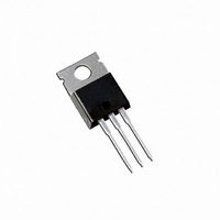
IRLB8748PBF International Rectifier, IRLB8748PBF Datasheet

IRLB8748PBF
Specifications of IRLB8748PBF
Available stocks
Related parts for IRLB8748PBF
IRLB8748PBF Summary of contents
Page 1
... Gate Parameter @ 10V (Silicon Limited 10V (Silicon Limited 10V (Package Limited Parameter g IRLB8748PbF ® HEXFET Power MOSFET R max Qg DS(on) 4.8m 15nC TO-220AB IRLB8748PbF D S Drain Source Max. Units 30 V ± 370 0.5 W/°C - 175 °C 300 (1.6mm from case lbf in (1.1N m) Typ ...
Page 2
... IRLB8748PbF Static @ T = 25°C (unless otherwise specified) J Parameter BV Drain-to-Source Breakdown Voltage DSS ∆ΒV /∆T Breakdown Voltage Temp. Coefficient DSS J R Static Drain-to-Source On-Resistance DS(on) V Gate Threshold Voltage GS(th) ∆V /∆T Gate Threshold Voltage Coefficient GS(th Drain-to-Source Leakage Current DSS I Gate-to-Source Forward Leakage ...
Page 3
... Fig 2. Typical Output Characteristics 2 40A 1 10V 1.6 1.4 1.2 1.0 0.8 0.6 0.4 -60 -40 - 100120140160180 Fig 4. Normalized On-Resistance IRLB8748PbF VGS 10V 9.0V 7.0V 5.5V 4.5V 4.0V 3.5V 3.0V 3.0V ≤ 60µs PULSE WIDTH Tj = 175° Drain-to-Source Voltage ( Junction Temperature (°C) vs ...
Page 4
... IRLB8748PbF 10000 0V MHZ C iss = SHORTED C rss = oss = iss 1000 C oss C rss 100 Drain-to-Source Voltage (V) Fig 5. Typical Capacitance vs. Drain-to-Source Voltage 1000 100 175° 25°C 1 0.1 0.0 0.5 1 Source-to-Drain Voltage (V) Fig 7. Typical Source-Drain Diode Forward Voltage 4 14 32A 12.0 10.0 8.0 6.0 4 ...
Page 5
... τ J τ J τ τ τ 1 τ τ Ci= τi/Ri Ci i/Ri 0.0001 0.001 Rectangular Pulse Duration (sec) IRLB8748PbF 50µ 250µ 1.0mA 100 125 150 175 Temperature ( ° (°C/W) τi (sec 1.55246 0.005303 3 4 τ C τ 0.00682 8.250407 τ 4 τ τ 0.00172 6.932919 ...
Page 6
... IRLB8748PbF GS, Gate -to -Source Voltage (V) Fig 12. On-Resistance vs. Gate Voltage D.U 20V V GS 0.01 Ω Fig 13a. Unclamped Inductive Test Circuit Fig 13b. Unclamped Inductive Waveforms 6 500 40A 450 400 350 300 250 200 125°C 150 100 25° Starting Junction Temperature (°C) Fig 13c ...
Page 7
... D.U.T. V Waveform DS Re-Applied G + Voltage - Inductor Curent ® HEXFET Power MOSFETs Id Vgs + V DS D.U. Fig 17. Gate Charge Waveform IRLB8748PbF P.W. Period D = Period V =10V GS Body Diode Forward Current di/dt Diode Recovery dv/ Body Diode Forward Drop I Ripple ≤ for N-Channel Vds Vgs(th) Qgs1 ...
Page 8
... IRLB8748PbF TO-220AB packages are not recommended for Surface Mount Application. Note: For the most current drawing please refer to IR website at: http://www.irf.com/package/ 8 www.irf.com ...
Page 9
... This is only applied to TO-220AB pakcage. Data and specifications subject to change without notice. This product has been designed and qualified for the Industrial market. Qualification Standards can be found on IR’s Web site. Visit us at www.irf.com for sales contact information.04/2009 IRLB8748PbF TAC Fax: (310) 252-7903 9 ...


