IRFP3415PBF International Rectifier, IRFP3415PBF Datasheet
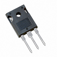
MOSFET N-CH 150V 43A TO-247AC

IRFP3415PBF

Manufacturer Part Number
IRFP3415PBF
Description
MOSFET N-CH 150V 43A TO-247AC
Manufacturer
International Rectifier
Series
HEXFET®r
Datasheets

Specifications of IRFP3415PBF

Fet Type
MOSFET N-Channel, Metal Oxide
Fet Feature
Standard
Rds On (max) @ Id, Vgs
42 mOhm @ 22A, 10V
Drain To Source Voltage (vdss)
150V
Current - Continuous Drain (id) @ 25° C
43A
Vgs(th) (max) @ Id
4V @ 250µA
Gate Charge (qg) @ Vgs
200nC @ 10V
Input Capacitance (ciss) @ Vds
2400pF @ 25V
Power - Max
200W
Mounting Type
Through Hole
Package / Case
TO-247-3 (Straight Leads), TO-247AC
Channel Type
N
Current, Drain
43 A
Gate Charge, Total
200 nC
Package Type
TO-247AC
Polarization
N-Channel
Power Dissipation
200 W
Resistance, Drain To Source On
0.042 Ohm
Resistance, Thermal, Junction To Case
0.75 °C/W
Temperature, Operating, Maximum
+175 °C
Temperature, Operating, Minimum
-55 °C
Time, Turn-off Delay
71 ns
Time, Turn-on Delay
12 ns
Transconductance, Forward
19 S
Voltage, Breakdown, Drain To Source
150 V
Voltage, Drain To Source
150 V
Voltage, Forward, Diode
1.3 V
Voltage, Gate To Source
±20 V
Transistor Polarity
N-Channel
Drain-source Breakdown Voltage
150 V
Gate-source Breakdown Voltage
20 V
Continuous Drain Current
43 A
Mounting Style
Through Hole
Gate Charge Qg
133.3 nC
Lead Free Status / RoHS Status
Lead free / RoHS Compliant
Other names
*IRFP3415PBF

Available stocks

Company
Part Number
Manufacturer
Quantity
Price
Company:
Part Number:
IRFP3415PBF
Quantity:
9 000
Company:
Part Number:
IRFP3415PBF M
Quantity:
5 000
www.irf.com
l
l
l
l
l
l
Description
Absolute Maximum Ratings
Thermal Resistance
Fifth Generation HEXFET
International Rectifier utilize advanced processing
techniques to achieve extremely low on-resistance per
silicon area. This benefit, combined with the fast
switching speed and ruggedized device design that
HEXFET power MOSFETs are well known for, provides
the designer with an extremely efficient and reliable
device for use in a wide variety of applications.
The TO-247 package is preferred for commercial-
industrial applications where higher power levels
preclude the use of TO-220 devices. The TO-247 is
similar but superior to the earlier TO-218 package
because of its isolated mounting hole.
I
I
I
P
V
E
I
E
dv/dt
T
T
R
R
R
D
D
DM
AR
J
STG
D
GS
AS
AR
θJC
θJA
θCS
@ T
@ T
@T
Advanced Process Technology
Dynamic dv/dt Rating
175°C Operating Temperature
Fast Switching
Fully Avalanche Rated
Lead-Free
C
C
C
= 25°C
= 100°C
= 25°C
Continuous Drain Current, V
Pulsed Drain Current 
Power Dissipation
Linear Derating Factor
Gate-to-Source Voltage
Single Pulse Avalanche Energy‚
Avalanche Current
Repetitive Avalanche Energy
Peak Diode Recovery dv/dt ƒ
Operating Junction and
Storage Temperature Range
Soldering Temperature, for 10 seconds
Mounting torque, 6-32 or M3 srew
Junction-to-Case
Case-to-Sink, Flat, Greased Surface
Junction-to-Ambient
®
Power MOSFETs from
Parameter
Parameter
GS
GS
@ 10V
@ 10V
G
Typ.
0.24
300 (1.6mm from case )
IRFP3415PbF
–––
–––
HEXFET
10 lbf•in (1.1N•m)
-55 to + 175
TO-247AC
D
S
Max.
± 20
590
200
1.3
5.0
43
30
22
20
®
R
Power MOSFET
DS(on)
V
Max.
0.75
–––
DSS
40
I
D
= 43A
= 0.042Ω
= 150V
Units
Units
°C/W
W/
V/ns
mJ
mJ
°C
W
A
V
A
1

Related parts for IRFP3415PBF

IRFP3415PBF Summary of contents

Page 1

... Storage Temperature Range STG Soldering Temperature, for 10 seconds Mounting torque, 6- srew Thermal Resistance Parameter R Junction-to-Case θJC R Case-to-Sink, Flat, Greased Surface θCS R Junction-to-Ambient θJA www.irf.com IRFP3415PbF HEXFET TO-247AC Max. @ 10V GS @ 10V GS - 175 300 (1.6mm from case ) 10 lbf•in (1.1N•m) Typ. ––– ...

Page 2

... IRFP3415PbF Electrical Characteristics @ T Parameter V Drain-to-Source Breakdown Voltage (BR)DSS ∆V Breakdown Voltage Temp. Coefficient /∆T (BR)DSS J R Static Drain-to-Source On-Resistance DS(on) V Gate Threshold Voltage GS(th) g Forward Transconductance fs Gate-to-Source Forward Leakage Gate-to-Source Reverse Leakage Q Total Gate Charge g Q Gate-to-Source Charge gs Q Gate-to-Drain ("Miller") Charge ...

Page 3

... TOP BOTTOM 100 o 10 100 1 3 2.5 2.0 1.5 ° J 1.0 0.5 = 50V 0.0 -60 -40 - IRFP3415PbF VGS 15V 10V 8.0V 7.0V 6.0V 5.5V 5.5V 4.5V 4.5V 20us PULSE WIDTH 175 Drain-to-Source Voltage (V) DS 37A V = 10V 100 120 140 160 180 ...

Page 4

... IRFP3415PbF 6000 1MHz iss rss gd 5000 oss ds gd 4000 C iss 3000 2000 C oss C rss 1000 Drain-to-Source Voltage (V) DS 1000 100 T = 175 0.1 0.2 0.6 1.0 V ,Source-to-Drain Voltage ( SHORTED 100 0 1000 OPERATION IN THIS AREA LIMITED 100 175 Single Pulse 1.4 1.8 ...

Page 5

... Fig 11. Maximum Effective Transient Thermal Impedance, Junction-to-Case www.irf.com Fig 10a. Switching Time Test Circuit V DS 90% 150 175 ° 10 d(on) Fig 10b. Switching Time Waveforms Notes: 1. Duty factor Peak 0.001 0. Rectangular Pulse Duration (sec) 1 IRFP3415PbF + - ≤ 1 ≤ 0 d(off thJC C ...

Page 6

... IRFP3415PbF D.U 20V 0.01 Ω Fig 12a. Unclamped Inductive Test Circuit Fig 12b. Unclamped Inductive Waveforms Charge Fig 13a. Basic Gate Charge Waveform 6 1400 1200 15V 1000 DRIVER 800 + V DD 600 - A 400 200 0 25 Starting T , Junction Temperature ( C) V (BR)DSS Fig 12c. Maximum Avalanche Energy Same Type as D ...

Page 7

... R G • Driver same type as D.U.T. • I controlled by Duty Factor "D" SD • D.U.T. - Device Under Test P.W. Period D = Period Body Diode Forward Current di/dt Diode Recovery dv/dt Body Diode Forward Drop Ripple ≤ 5% ® Power MOSFETs IRFP3415PbF + =10V ...

Page 8

... IRFP3415PbF EXAMPLE: THIS IS AN IRFPE30 WITH AS SEMBLY LOT CODE 5657 ASS EMBLED ON WW 35, 2000 IN THE AS SEMBLY LINE "H" Note: "P" in assembly line position indicates "Lead-Free" IR WORLD HEADQUARTERS: 233 Kansas St., El Segundo, California 90245, USA Tel: (310) 252-7105 8 INTERNATIONAL RECTIFIER IRFPE30 LOGO ...

Page 9

Note: For the most current drawings please refer to the IR website at: http://www.irf.com/package/ ...

Related keywords