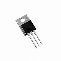
IRFB52N15DPBF International Rectifier, IRFB52N15DPBF Datasheet

IRFB52N15DPBF
Specifications of IRFB52N15DPBF
Available stocks
Related parts for IRFB52N15DPBF
IRFB52N15DPBF Summary of contents
Page 1
... Notes through ‡ are on page 11 www.irf.com min. DS (Avalanche) R max @ 10V DS(ON) T max J to Simplify TO-220AB IRFB52N15DPbF @ 10V ‡ 10V ‡ 97002A HEXFET Power MOSFET Key Parameters 150 200 m 32 175 2 D Pak TO-262 ...
Page 2
... IRFB52N15DPbF/IRFS52N15DPbF/IRFSL52N15DPbF Static @ T = 25°C (unless otherwise specified) J Parameter V Drain-to-Source Breakdown Voltage (BR)DSS Breakdown Voltage Temp. Coefficient (BR)DSS J R Static Drain-to-Source On-Resistance DS(on) V Gate Threshold Voltage GS(th) I Drain-to-Source Leakage Current DSS Gate-to-Source Forward Leakage I GSS Gate-to-Source Reverse Leakage Dynamic @ T = 25°C (unless otherwise specified) ...
Page 3
... Drain-to-Source Voltage (V) Fig 1. Typical Output Characteristics 1000.00 100. 25°C 10. 15V 300µs PULSE WIDTH 1.00 5.0 7.0 9.0 11 Gate-to-Source Voltage (V) Fig 3. Typical Transfer Characteristics www.irf.com IRFB52N15DPbF/IRFS52N15DPbF/IRFSL52N15DPbF 1000 TOP 100 BOTTOM 5.0V 10 5.0V 1 0.1 10 100 0.1 Fig 2. Typical Output Characteristics 3 2.5 2 175° ...
Page 4
... IRFB52N15DPbF/IRFS52N15DPbF/IRFSL52N15DPbF 100000 0V, C iss = rss = oss = 10000 Ciss 1000 Coss 100 Crss Drain-to-Source Voltage (V) Fig 5. Typical Capacitance Vs. Drain-to-Source Voltage 1000.00 100. 175°C 10. 25°C 1.00 0.10 0.0 0.5 1.0 1 Source-toDrain Voltage (V) Fig 7. Typical Source-Drain Diode Forward Voltage 36A MHZ SHORTED ...
Page 5
... D = 0.50 0.20 0.1 0.10 0.05 SINGLE PULSE 0.02 0.01 (THERMAL RESPONSE) 0.01 0.001 0.00001 0.0001 Fig 11. Maximum Effective Transient Thermal Impedance, Junction-to-Case www.irf.com IRFB52N15DPbF/IRFS52N15DPbF/IRFSL52N15DPbF Fig 10a. Switching Time Test Circuit V DS 90% 125 150 175 ° 10 Fig 10b. Switching Time Waveforms 0.001 ...
Page 6
... IRFB52N15DPbF/IRFS52N15DPbF/IRFSL52N15DPbF D.U 20V 0. Fig 12a. Unclamped Inductive Test Circuit V (BR)DSS Fig 12b. Unclamped Inductive Waveforms Charge Fig 13a. Basic Gate Charge Waveform 6 900 15V 720 DRIVER + 540 360 180 Starting Tj, Junction Temperature Fig 12c. Maximum Avalanche Energy Fig 13b. Gate Charge Test Circuit ...
Page 7
... Driver Gate Drive P.W. D.U.T. I Waveform SD Reverse Recovery Current D.U.T. V Waveform DS Re-Applied Voltage Inductor Curent Fig 14. For N-Channel HEXFET www.irf.com IRFB52N15DPbF/IRFS52N15DPbF/IRFSL52N15DPbF + ƒ - „ P.W. Period D = Period Body Diode Forward Current di/dt Diode Recovery dv/dt Body Diode Forward Drop Ripple 5% ® ...
Page 8
... IRFB52N15DPbF/IRFS52N15DPbF/IRFSL52N15DPbF EXAMPLE: T HIS IS AN IRF1010 LOT CODE 1789 AS S EMBLED ON WW 19, 1997 IN THE AS SEMBLY LINE "C" Note: "P" inass embly line position indicates "Lead - Free" TO-220 package is not recommended for Surface Mount Application. Notes: 1. For an Automotive Qualified version of this part please see http://www.irf.com/product-info/auto/ 2 ...
Page 9
... AS SEMBLED ON WW 02, 2000 EMBLY LINE "L" OR Notes: 1. For an Automotive Qualified version of this part please see http://www.irf.com/product-info/auto/ 2. For the most current drawing please refer to IR website at http://www.irf.com/package/ www.irf.com IRFB52N15DPbF/IRFS52N15DPbF/IRFSL52N15DPbF INT ERNAT IONAL RECT IFIER F530S LOGO AS S EMBLY LOT CODE ...
Page 10
... IRFB52N15DPbF/IRFS52N15DPbF/IRFSL52N15DPbF TO-262 Package Outline TO-262 Part Marking Information EXAMPLE: T HIS IS AN IRL3103L LOT CODE 1789 ASS EMBLED ON WW 19, 1997 ASSEMBLY LINE "C" Notes: 1. For an Automotive Qualified version of this part please see http://www.irf.com/product-info/auto/ 2. For the most current drawing please refer to IR website at http://www.irf.com/package/ ...
Page 11
... T 175°C. J „ Pulse width 300µs; duty cycle 2%. IR WORLD HEADQUARTERS: 233 Kansas St., El Segundo, California 90245, USA Tel: (310) 252-7105 www.irf.com IRFB52N15DPbF/IRFS52N15DPbF/IRFSL52N15DPbF 1.60 (.063) 1.50 (.059) 4.10 (.161) 3.90 (.153) 11.60 (.457) 1.85 (.073) 11.40 (.449) 1.65 (.065) 1.75 (.069) 10 ...


