NTLJS1102PTAG ON Semiconductor, NTLJS1102PTAG Datasheet
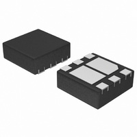
MOSFET P-CH 8V 3.7A 6-WDFN

NTLJS1102PTAG

Manufacturer Part Number
NTLJS1102PTAG
Description
MOSFET P-CH 8V 3.7A 6-WDFN
Manufacturer
ON Semiconductor
Datasheet

Specifications of NTLJS1102PTAG

Fet Type
MOSFET P-Channel, Metal Oxide
Fet Feature
Logic Level Gate
Rds On (max) @ Id, Vgs
36 mOhm @ 6.2A, 4.5V
Drain To Source Voltage (vdss)
8V
Current - Continuous Drain (id) @ 25° C
3.7A
Vgs(th) (max) @ Id
720mV @ 250µA
Gate Charge (qg) @ Vgs
25nC @ 4.5V
Input Capacitance (ciss) @ Vds
1585pF @ 4V
Power - Max
700mW
Mounting Type
Surface Mount
Package / Case
6-VDFN Exposed Pad
Configuration
Single Quad Drain
Transistor Polarity
P-Channel
Resistance Drain-source Rds (on)
80 mOhms
Forward Transconductance Gfs (max / Min)
14.3 S
Drain-source Breakdown Voltage
- 8 V
Gate-source Breakdown Voltage
+/- 6 V
Continuous Drain Current
6.2 A
Power Dissipation
3.3 W
Maximum Operating Temperature
+ 150 C
Mounting Style
SMD/SMT
Minimum Operating Temperature
- 55 C
Lead Free Status / RoHS Status
Lead free / RoHS Compliant
NTLJS1102P
Power MOSFET
−8 V, −8.1 A, mCOOL] Single P−Channel,
2x2 mm, WDFN package
Features
Applications
1. Surface−mounted on FR4 board using 1 in sq pad size (Cu area = 1.127 in sq
2. Surface−mounted on FR4 board using the minimum recommended pad size
© Semiconductor Components Industries, LLC, 2008
November, 2008 − Rev. 0
MAXIMUM RATINGS
Drain−to−Source Voltage
Gate−to−Source Voltage
Continuous
Drain Current
(Note 1)
Power
Dissipation
(Note 1)
Continuous
Drain Current
(Note 2)
Power
Dissipation
(Note 2)
Pulsed Drain Current
Operating Junction and Storage
Temperature
Source Current (Body Diode) (Note 2)
Lead Temperature for Soldering Purposes
(1/8″ from case for 10 s)
Conduction
Drive
Portable Equipment
WDFN Package with Exposed Drain Pad for Excellent Thermal
Lowest R
1.2 V R
2 x 2 mm Footprint Same as SC−88 Package
Low Profile (<0.8 mm) for Easy Fit in Thin Environments
This is a Halide−Free Device
This is a Pb−Free Device
High Side Load Switch
Li Ion Battery Linear Mode Charging
Optimized for Battery and Load Management Applications in
[2 oz] including traces).
(Cu area = 30 mm
DS(on)
DS(on)
Parameter
Rating for Operation at Low Voltage Logic Level Gate
in 2 x 2 mm Package
2
Steady
t v 5 s
Steady
t v 5 s
Steady
State
State
State
[2 oz] including traces).
(T
J
= 25°C unless otherwise stated)
T
T
T
T
T
T
T
t
p
A
A
A
A
A
A
A
= 10 ms
= 25°C
= 85°C
= 25°C
= 25°C
= 25°C
= 85°C
= 25°C
T
Symbol
J
V
V
, T
I
P
P
DSS
DM
T
I
I
I
GS
D
D
S
D
D
L
STG
−55 to
Value
−6.2
−4.5
−8.1
−3.7
−2.7
−5.5
−30
150
260
± 6
1.9
3.3
0.7
−8
1
Unit
°C
°C
W
W
V
V
A
A
A
A
See detailed ordering and shipping information in the package
dimensions section on page 3 of this data sheet.
Pin 1
V
S
−8.0 V
(BR)DSS
J6
M
G
(Note: Microdot may be in either location)
G
D
D
ORDERING INFORMATION
= Specific Device Code
= Date Code
= Pb−Free Package
1
2
3
G
300 mW @ −1.2 V
PIN CONNECTIONS
36 mW @ −4.5 V
45 mW @ −2.5 V
68 mW @ −1.8 V
90 mW @ −1.5 V
http://onsemi.com
P−CHANNEL MOSFET
R
D
DS(on)
(Top View)
CASE 506AP
WDFN6
MAX
S
D
Publication Order Number:
D
S
NTLJS1102P/D
6
5
4
MARKING
DIAGRAM
1
2
3
I
D
−6.2 A
−5.5 A
−3.0 A
−1.0 A
−0.2 A
J6MG
MAX
D
D
S
G
6
5
4

Related parts for NTLJS1102PTAG

NTLJS1102PTAG Summary of contents

Page 1

NTLJS1102P Power MOSFET −8 V, −8.1 A, mCOOL] Single P−Channel, 2x2 mm, WDFN package Features • WDFN Package with Exposed Drain Pad for Excellent Thermal Conduction • Lowest Package DS(on) • 1 ...

Page 2

THERMAL RESISTANCE RATINGS Parameter Junction−to−Ambient – Steady State (Note 3) Junction−to−Ambient – (Note 3) Junction−to−Ambient – Steady State min Pad (Note 4) 3. Surface−mounted on FR4 board using pad size (Cu area = ...

Page 3

... Pulse Test: pulse width v 300 ms, duty cycle Switching characteristics are independent of operating junction temperatures ORDERING INFORMATION Device NTLJS1102PTBG NTLJS1102PTAG †For information on tape and reel specifications, including part orientation and tape sizes, please refer to our Tape and Reel Packaging Specifications Brochure, BRD8011/ 25°C unless otherwise specified) ...

Page 4

V −2 0.5 1.0 1.5 2.0 2.5 3.0 −V , DRAIN−TO−SOURCE VOLTAGE (V) DS Figure 1. On−Region Characteristics 0.20 0.18 0.16 0.14 0.12 0. −6.2 A ...

Page 5

C iss 2000 1800 1600 1400 1200 C oss 1000 800 600 400 C rss 200 −V , DRAIN−TO−SOURCE VOLTAGE (V) DS Figure 7. Capacitance Variation 1000 V = −4.5 V ...

Page 6

V GS Single Pulse 0.1 0.1 Figure 13. Maximum Rated Forward Biased 1 Duty Cycle = 0.5 0.2 0.1 0.1 0.05 Single Pulse 0.01 1E−04 1E−03 1E−02 TYPICAL CHARACTERISTICS = − 25°C 100 ...

Page 7

... C NOTE 3 0.65 PITCH *For additional information on our Pb−Free strategy and soldering details, please download the ON Semiconductor Soldering and Mounting Techniques Reference Manual, SOLDERRM/D. N. American Technical Support: 800−282−9855 Toll Free USA/Canada Europe, Middle East and Africa Technical Support: Phone: 421 33 790 2910 Japan Customer Focus Center Phone: 81− ...

Related keywords