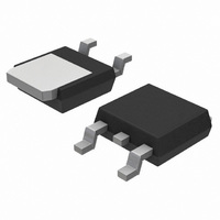
MTD5P06VT4G ON Semiconductor, MTD5P06VT4G Datasheet - Page 2

MTD5P06VT4G
Manufacturer Part Number
MTD5P06VT4G
Description
MOSFET P-CH 60V 5A DPAK
Manufacturer
ON Semiconductor
Datasheet
1.MTD5P06VT4G.pdf
(7 pages)
Specifications of MTD5P06VT4G
Fet Type
MOSFET P-Channel, Metal Oxide
Fet Feature
Standard
Rds On (max) @ Id, Vgs
450 mOhm @ 2.5A, 10V
Drain To Source Voltage (vdss)
60V
Current - Continuous Drain (id) @ 25° C
5A
Vgs(th) (max) @ Id
4V @ 250µA
Gate Charge (qg) @ Vgs
20nC @ 10V
Input Capacitance (ciss) @ Vds
510pF @ 25V
Power - Max
40W
Mounting Type
Surface Mount
Package / Case
DPak, TO-252 (2 leads+tab), SC-63
Configuration
Single
Transistor Polarity
P-Channel
Resistance Drain-source Rds (on)
0.45 Ohm @ 10 V
Forward Transconductance Gfs (max / Min)
3.6 S
Drain-source Breakdown Voltage
60 V
Gate-source Breakdown Voltage
+/- 15 V
Continuous Drain Current
5 A
Power Dissipation
2100 mW
Maximum Operating Temperature
+ 175 C
Mounting Style
SMD/SMT
Minimum Operating Temperature
- 55 C
Lead Free Status / RoHS Status
Lead free / RoHS Compliant
Other names
MTD5P06VT4GOS
MTD5P06VT4GOS
MTD5P06VT4GOSTR
MTD5P06VT4GOS
MTD5P06VT4GOSTR
Available stocks
Company
Part Number
Manufacturer
Quantity
Price
Company:
Part Number:
MTD5P06VT4G
Manufacturer:
DIODES
Quantity:
43 000
Company:
Part Number:
MTD5P06VT4G
Manufacturer:
ON
Quantity:
12 500
Company:
Part Number:
MTD5P06VT4G
Manufacturer:
ON SEMICONDUCTOR
Quantity:
30 000
3. Pulse Test: Pulse Width ≤ 300 ms, Duty Cycle ≤ 2%.
4. Switching characteristics are independent of operating junction temperature.
ELECTRICAL CHARACTERISTICS
OFF CHARACTERISTICS
ON CHARACTERISTICS (Note 3)
DYNAMIC CHARACTERISTICS
SWITCHING CHARACTERISTICS (Note 4)
SOURCE−DRAIN DIODE CHARACTERISTICS
INTERNAL PACKAGE INDUCTANCE
Drain−Source Breakdown Voltage
Temperature Coefficient (Positive)
Zero Gate Voltage Drain Current
Gate−Body Leakage Current (V
Gate Threshold Voltage
Threshold Temperature Coefficient (Negative)
Static Drain−Source On−Resistance (V
Drain−Source On−Voltage
Forward Transconductance
Input Capacitance
Output Capacitance
Transfer Capacitance
Turn−On Delay Time
Rise Time
Turn−Off Delay Time
Fall Time
Gate Charge
(See Figure 8)
Forward On−Voltage
Reverse Recovery Time
Reverse Recovery Stored Charge
Internal Drain Inductance
Internal Source Inductance
(V
(V
(V
(V
(V
(V
(V
(Measured from the drain lead 0.25″ from package to center of die)
(Measured from the source lead 0.25″ from package to source bond pad)
GS
DS
DS
DS
GS
GS
DS
= 0 Vdc, I
= 60 Vdc, V
= 60 Vdc, V
= V
= 10 Vdc, I
= 10 Vdc, I
= 15 Vdc, I
GS
, I
D
D
= 250 mAdc)
D
D
D
= 0.25 mAdc)
GS
GS
= 2.5 Adc)
= 5 Adc)
= 2.5 Adc, T
= 0 Vdc)
= 0 Vdc, T
GS
J
J
= ± 15 Vdc, V
Characteristic
= 150°C)
= 150°C)
GS
(V
(T
(I
DS
= 10 Vdc, I
S
J
= 5 Adc, V
= 25°C unless otherwise noted)
= 48 Vdc, I
(V
V
(V
(I
(I
DS
DS
GS
S
S
DD
= 5 Adc, V
= 5 Adc, V
= 0 Vdc)
= 25 Vdc, V
dI
= 10 Vdc, R
= 30 Vdc, I
D
S
f = 1.0 MHz)
/dt = 100 A/ms)
= 2.5 Adc)
GS
D
http://onsemi.com
= 5 Adc, V
= 0 Vdc, T
MTD5P06V
GS
GS
GS
D
G
= 0 Vdc)
= 0 Vdc,
= 5 Adc,
= 9.1 W)
= 0 Vdc,
2
GS
J
= 150°C)
= 10 Vdc)
V
Symbol
R
V
V
(BR)DSS
t
t
I
I
DS(on)
C
Q
GS(th)
DS(on)
C
C
V
g
d(on)
d(off)
GSS
DSS
Q
Q
Q
Q
L
L
t
t
t
oss
t
t
FS
SD
RR
iss
rss
rr
a
b
r
f
D
S
T
1
2
3
Min
2.0
1.5
60
−
−
−
−
−
−
−
−
−
−
−
−
−
−
−
−
−
−
−
−
−
−
−
−
−
−
−
61.2
0.34
1.72
1.34
0.42
Typ
367
140
2.8
4.7
3.6
3.0
5.0
5.0
4.5
7.5
29
11
26
17
19
12
97
73
24
−
−
−
−
−
−
Max
0.45
100
100
510
200
4.0
2.7
2.6
3.5
10
60
20
50
30
40
20
−
−
−
−
−
−
−
−
−
−
−
−
−
−
mV/°C
mV/°C
Mhos
mAdc
nAdc
Unit
Vdc
Vdc
Vdc
Vdc
nC
mC
nH
nH
pF
ns
ns
W


