NDD02N60Z-1G ON Semiconductor, NDD02N60Z-1G Datasheet

MOSFET N-CH 600V IPAK

NDD02N60Z-1G

Manufacturer Part Number
NDD02N60Z-1G
Description
MOSFET N-CH 600V IPAK
Manufacturer
ON Semiconductor
Datasheet

Specifications of NDD02N60Z-1G

Package / Case
IPak, TO-251 (2 straight leads + tab)
Mounting Type
Through Hole
Power - Max
57W
Fet Type
MOSFET N-Channel, Metal Oxide
Gate Charge (qg) @ Vgs
10.1nC @ 10V
Vgs(th) (max) @ Id
4.5V @ 50µA
Current - Continuous Drain (id) @ 25° C
2.2A
Drain To Source Voltage (vdss)
600V
Fet Feature
Standard
Rds On (max) @ Id, Vgs
4.8 Ohm @ 1A, 10V
Configuration
Single
Transistor Polarity
N-Channel
Resistance Drain-source Rds (on)
4 Ohms
Forward Transconductance Gfs (max / Min)
1.7 S
Drain-source Breakdown Voltage
600 V
Gate-source Breakdown Voltage
30 V
Continuous Drain Current
1.4 A
Power Dissipation
57 W
Maximum Operating Temperature
+ 125 C
Mounting Style
Through Hole
Gate Charge Qg
10.1 nC
Minimum Operating Temperature
- 55 C
Lead Free Status / RoHS Status
Lead free / RoHS Compliant

Available stocks

Company
Part Number
Manufacturer
Quantity
Price
Part Number:
NDD02N60Z-1G
Manufacturer:
ON
Quantity:
3 225
Part Number:
NDD02N60Z-1G
Manufacturer:
ON Semiconductor
Quantity:
15
Part Number:
NDD02N60Z-1G
Manufacturer:
ON
Quantity:
12 500
Company:
Part Number:
NDD02N60Z-1G
Quantity:
2 000
Company:
Part Number:
NDD02N60Z-1G
Quantity:
125
NDF02N60Z, NDP02N60Z,
NDD02N60Z
N-Channel Power MOSFET
600 V, 4.0 W
Features
Stresses exceeding Maximum Ratings may damage the device. Maximum
Ratings are stress ratings only. Functional operation above the Recommended
Operating Conditions is not implied. Extended exposure to stresses above the
Recommended Operating Conditions may affect device reliability.
1. Limited by maximum junction temperature
2. I
ABSOLUTE MAXIMUM RATINGS
© Semiconductor Components Industries, LLC, 2010
April, 2010 − Rev. 2
Drain−to−Source Voltage
Continuous Drain Current
R
Continuous Drain Current
R
Pulsed Drain Current, V
@ 10 V
Power Dissipation R
Gate−to−Source Voltage
Single Pulse Avalanche
Energy, I
ESD (HBM)
(JESD 22−A114)
RMS Isolation Voltage
(t = 0.3 sec., R.H. ≤ 30%,
T
Peak Diode Recovery
Continuous Source Current
(Body Diode)
Maximum Temperature for
Soldering Leads
Operating Junction and
Storage Temperature Range
A
Low ON Resistance
Low Gate Charge
100% Avalanche Tested
These Devices are Pb−Free and are RoHS Compliant
qJC
qJC
SD
= 25°C) (Figure 17)
T
= 2.4 A, di/dt ≤ 100 A/ms, V
A
= 100°C
D
Rating
= 2.4 A
qJC
GS
Symbol
T
V
V
dv/dt
V
J
V
E
I
P
DD
DSS
T
, T
DM
I
I
ISO
I
esd
GS
AS
D
D
S
D
L
stg
≤ BV
(T
C
DSS
(Note 1)
(Note 1)
(Note 1)
= 25°C unless otherwise noted)
4500
NDF
2.4
1.6
10
24
, T
J
4.5 (Note 2)
= +150°C
−55 to 150
2500
600
120
260
2.4
NDP
30
2.4
1.6
10
72
NDD
2.2
1.4
57
9
1
V/ns
Unit
mJ
°C
°C
W
V
A
A
A
V
V
V
A
CASE 221D
See detailed ordering and shipping information in the package
dimensions section on page 7 of this data sheet.
TO−220FP
MARKING AND ORDERING INFORMATION
1
STYLE 1
2
3
600 V
V
DSS
G (1)
CASE 221A
1
TO−220AB
STYLE 5
http://onsemi.com
2
3
N−Channel
CASE 369D
Publication Order Number:
D (2)
R
STYLE 2
1
DS(on)
IPAK
2
3
S (3)
4.0 W
(TYP) @ 1 A
NDF02N60Z/D
4
CASE 369AA
1 2
STYLE 2
DPAK
3
4

Related parts for NDD02N60Z-1G

NDD02N60Z-1G Summary of contents

Page 1

... NDF02N60Z, NDP02N60Z, NDD02N60Z N-Channel Power MOSFET 600 V, 4.0 W Features • Low ON Resistance • Low Gate Charge • 100% Avalanche Tested • These Devices are Pb−Free and are RoHS Compliant ABSOLUTE MAXIMUM RATINGS (T Rating Symbol Drain−to−Source Voltage V DSS Continuous Drain Current ...

Page 2

... SOURCE−DRAIN DIODE CHARACTERISTICS (T Diode Forward Voltage Reverse Recovery Time Reverse Recovery Charge 5. Pulse Width ≤ 380 ms, Duty Cycle ≤ 2%. NDP02N60Z NDF02N60Z NDD02N60Z (Note 3) NDP02N60Z (Note 3) NDF02N60Z (Note 4) NDD02N60Z (Note 3) NDD02N60Z− 25°C unless otherwise noted) J Test Conditions Reference to 25°C, ...

Page 3

V 3 2.5 2.0 1.5 1.0 0.5 0.0 0.0 5.0 10.0 15 DRAIN−TO−SOURCE VOLTAGE (V) DS Figure 1. On−Region Characteristics 6.00 5.75 5.50 5.25 5.00 4.75 4.50 4.25 4.00 3.75 ...

Page 4

T = 150° 125° 100 150 200 250 300 350 400 450 500 550 600 V , DRAIN−TO−SOURCE VOLTAGE (V) DS Figure 7. Drain−to−Source Leakage Current versus Voltage 15.0 14.0 13.0 ...

Page 5

... Figure 14. Thermal Impedance (Junction−to−Case) for NDD02N60Z 100 50% (DUTY CYCLE) 10 20% 10% 5.0% 1 2.0% 1.0% 0.1 SINGLE PULSE 0.01 1E−06 1E−05 1E−04 Figure 15. Thermal Impedance (Junction−to−Ambient) for NDD02N60Z TYPICAL CHARACTERISTICS 100 V GS SINGLE PULSE 25° 0.1 LIMIT 0.01 100 1000 0 ...

Page 6

... Figure 16. Thermal Impedance (Junction−to−Case) for NDF02N60Z Measurement made between leads and heatsink with all leads shorted together. *For additional mounting information, please download the ON Semiconductor Soldering and Mounting Techniques Reference Manual, SOLDERRM/D. 1E−03 1E−02 1E−01 PULSE TIME (s) ...

Page 7

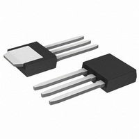
... ORDERING INFORMATION Order Number NDF02N60ZG NDP02N60ZG NDD02N60Z−1G NDD02N60ZT4G †For information on tape and reel specifications, including part orientation and tape sizes, please refer to our Tape and Reel Packaging Specifications Brochure, BRD8011/D. NDF02N60ZG or NDP02N60ZG AYWW Gate Drain Package TO−220FP (Pb−Free) TO−220AB (Pb−Free) IPAK (Pb− ...

Page 8

PACKAGE DIMENSIONS TO−220 FULLPAK −B− −Y− 0.25 (0.010 ...

Page 9

... 0.13 (0.005) M *For additional information on our Pb−Free strategy and soldering details, please download the ON Semiconductor Soldering and Mounting Techniques Reference Manual, SOLDERRM/D. PACKAGE DIMENSIONS IPAK CASE 369D−01 ISSUE DPAK CASE 369AA−01 ISSUE A SEATING −T− PLANE SOLDERING FOOTPRINT ...

Page 10

... Opportunity/Affirmative Action Employer. This literature is subject to all applicable copyright laws and is not for resale in any manner. PUBLICATION ORDERING INFORMATION LITERATURE FULFILLMENT: Literature Distribution Center for ON Semiconductor P.O. Box 5163, Denver, Colorado 80217 USA Phone: 303−675−2175 or 800−344−3860 Toll Free USA/Canada Fax: 303− ...

Related keywords