NDF04N60ZG ON Semiconductor, NDF04N60ZG Datasheet
NDF04N60ZG
Specifications of NDF04N60ZG
Available stocks


Related parts for NDF04N60ZG

NDF04N60ZG Summary of contents
Page 1
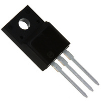
NDF04N60Z, NDP04N60Z, NDD04N60Z N-Channel Power MOSFET 600 V, 1.8 W Features • Low ON Resistance • Low Gate Charge • 100% Avalanche Tested • These Devices are Pb−Free and are RoHS Compliant ABSOLUTE MAXIMUM RATINGS (T Parameter Symbol Drain−to−Source Voltage ...
Page 2
THERMAL RESISTANCE Parameter Junction−to−Case (Drain) Junction−to−Ambient Steady State ELECTRICAL CHARACTERISTICS Characteristic OFF CHARACTERISTICS Drain−to−Source Breakdown Voltage Breakdown Voltage Temperature Coefficient Drain−to−Source Leakage Current Gate−to−Source Forward Leakage ON CHARACTERISTICS (Note 5) Static Drain−to−Source On−Resistance Gate Threshold Voltage Forward Transconductance DYNAMIC CHARACTERISTICS ...
Page 3
25° DRAIN−TO−SOURCE VOLTAGE (V) DS Figure 1. On−Region Characteristics 3.5 3 2 (V) GS Figure 3. On−Resistance ...
Page 4
C iss 600 400 C oss 200 C rss 100 V , DRAIN−TO−SOURCE VOLTAGE (V) DS Figure 7. Capacitance Variation 100 V = 300 ...
Page 5
... Figure 14. Thermal Impedance for NDD04N60Z Figure 15. Mounting Position for Isolation Test Measurement made between leads and heatsink with all leads shorted together. *For additional mounting information, please download the ON Semiconductor Soldering and Mounting Techniques Reference Manual, SOLDERRM/D. TYPICAL CHARACTERISTICS 0.001 ...
Page 6
... ORDERING INFORMATION Order Number NDF04N60ZG NDP04N60ZG NDD04N60Z−1G NDD04N60ZT4G †For information on tape and reel specifications, including part orientation and tape sizes, please refer to our Tape and Reel Packaging Specifications Brochure, BRD8011/D. NDF04N60ZG or NDP04N60ZG AYWW Gate Source Drain Package TO−220FP (Pb−Free) TO−220AB (Pb− ...
Page 7
PACKAGE DIMENSIONS TO−220 FULLPAK −B− −Y− 0.25 (0.010 ...
Page 8
−T− SEATING K PLANE 0.13 (0.005) M PACKAGE DIMENSIONS IPAK CASE 369D−01 ISSUE http://onsemi.com 8 NOTES: 1. DIMENSIONING AND ...
Page 9
... PL 0.13 (0.005) *For additional information on our Pb−Free strategy and soldering details, please download the ON Semiconductor Soldering and Mounting Techniques Reference Manual, SOLDERRM/D. ON Semiconductor and are registered trademarks of Semiconductor Components Industries, LLC (SCILLC). SCILLC reserves the right to make changes without further notice to any products herein ...