IRFP140N International Rectifier, IRFP140N Datasheet - Page 2
IRFP140N
Manufacturer Part Number
IRFP140N
Description
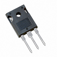
MOSFET N-CH 100V 33A TO-247AC
Manufacturer
International Rectifier
Series
HEXFET®r
Datasheet
1.IRFP140N.pdf
(9 pages)
Specifications of IRFP140N
Fet Type
MOSFET N-Channel, Metal Oxide
Fet Feature
Standard
Rds On (max) @ Id, Vgs
52 mOhm @ 16A, 10V
Drain To Source Voltage (vdss)
100V
Current - Continuous Drain (id) @ 25° C
33A
Vgs(th) (max) @ Id
4V @ 250µA
Gate Charge (qg) @ Vgs
94nC @ 10V
Input Capacitance (ciss) @ Vds
1400pF @ 25V
Power - Max
140W
Mounting Type
Through Hole
Package / Case
TO-247-3 (Straight Leads), TO-247AC
Lead Free Status / RoHS Status
Contains lead / RoHS non-compliant
Other names
*IRFP140N
Available stocks
Company
Part Number
Manufacturer
Quantity
Price
Company:

Part Number:
IRFP140N
Manufacturer:
FAIRCHILD
Quantity:
1 050
Part Number:
IRFP140N
Manufacturer:
IR
Quantity:
20 000
Part Number:
IRFP140NPBF
Manufacturer:
IR
Quantity:
20 000


IRFP140N
Electrical Characteristics @ T
Notes:
Source-Drain Ratings and Characteristics
I
I
I
I
V
t
Q
V
R
V
g
Q
Q
Q
t
t
t
t
L
C
C
C
L
DSS
GSS
SM
d(on)
r
d(off)
f
S
rr
V
D
fs
(BR)DSS
GS(th)
S
SD
DS(on)
iss
oss
rss
g
gs
gd
rr
Repetitive rating; pulse width limited by
V
(BR)DSS
R
2
max. junction temperature. ( See fig. 11 )
DD
G
= 25 , I
= 25V, starting T
/ T
J
Drain-to-Source Leakage Current
Continuous Source Current
(Body Diode)
Pulsed Source Current
(Body Diode)
Diode Forward Voltage
Reverse Recovery Time
Reverse RecoveryCharge
Drain-to-Source Breakdown Voltage
Breakdown Voltage Temp. Coefficient
Static Drain-to-Source On-Resistance
Gate Threshold Voltage
Forward Transconductance
Gate-to-Source Forward Leakage
Gate-to-Source Reverse Leakage
Total Gate Charge
Gate-to-Source Charge
Gate-to-Drain ("Miller") Charge
Turn-On Delay Time
Rise Time
Turn-Off Delay Time
Fall Time
Internal Drain Inductance
Input Capacitance
Output Capacitance
Reverse Transfer Capacitance
Internal Source Inductance
AS
= 16A. (See Figure 12)
J
= 25°C, L = 2.0mH
Parameter
Parameter
J
= 25°C (unless otherwise specified)
Pulse width
I
Uses IRF540N data and test conditions.
T
100
–––
–––
–––
–––
–––
–––
–––
–––
–––
–––
–––
–––
–––
–––
–––
–––
–––
–––
Min. Typ. Max. Units
2.0
Min. Typ. Max. Units
SD
–––
–––
–––
–––
11
–––
–––
J
175°C
16A, di/dt
1400 –––
0.11
–––
–––
–––
–––
–––
–––
–––
–––
–––
330
–––
–––
170
––– 0.052
–––
––– -100
170
8.2
1.1
5.0
39
44
33
13
–––
110
–––
–––
–––
250
–––
–––
250
100
–––
–––
–––
–––
300µs; duty cycle
4.0
–––
–––
1.3
1.6
25
94
43
33
15
210A/µs, V
V/°C
µA
nA
nC
nH
µC
ns
pF
ns
V
S
V
A
V
V
Reference to 25°C, I
V
V
V
V
V
V
I
V
V
I
R
Between lead,
6mm (0.25in.)
from package
and center of die contact
V
V
MOSFET symbol
showing the
integral reverse
p-n junction diode.
T
T
di/dt = 100A/µs
V
V
R
ƒ = 1.0MHz, See Fig. 5
D
D
DD
J
J
GS
GS
DS
DS
DS
DS
GS
GS
DS
GS
DD
GS
DS
G
D
= 16A
= 16A
= 25°C, I
= 25°C, I
= 3.0
= 5.1
= V
= 50V, I
= 100V, V
= 80V, V
= 80V
= 50V
= 25V
= 0V, I
= 10V, I
= 20V
= -20V
= 10V, See Fig. 6 and 13
= 0V
V
2%.
(BR)DSS
GS
, I
D
See Fig. 10
S
F
D
D
D
Conditions
= 250µA
GS
Conditions
= 16A, V
= 16A
= 250µA
= 16A
,
= 16A
GS
= 0V, T
= 0V
D
GS
= 1mA
J
= 150°C
= 0V
www.irf.com
G
G
S
D
D
S
Related parts for IRFP140N
Image
Part Number
Description
Manufacturer
Datasheet
Request
R

Part Number:
Description:
SCHOTTKY RECTIFIER
Manufacturer:
International Rectifier Corp.
Datasheet:
Part Number:
Description:
SCHOTTKY RECTIFIER
Manufacturer:
International Rectifier Corp.
Datasheet:
Part Number:
Description:
SCHOTTKY RECTIFIER
Manufacturer:
International Rectifier Corp.
Datasheet:
Part Number:
Description:
SCHOTTKY RECTIFIER
Manufacturer:
International Rectifier Corp.
Datasheet:
Part Number:
Description:
SCHOTTKY RECTIFIER
Manufacturer:
International Rectifier Corp.
Datasheet:
Part Number:
Description:
SCHOTTKY RECTIFIER
Manufacturer:
International Rectifier Corp.
Datasheet:
Part Number:
Description:
SCHOTTKY RECTIFIER
Manufacturer:
International Rectifier Corp.
Datasheet:
Part Number:
Description:
SCHOTTKY RECTIFIER
Manufacturer:
International Rectifier Corp.
Datasheet:
Part Number:
Description:
SCHOTTKY RECTIFIER
Manufacturer:
International Rectifier Corp.
Datasheet:
Part Number:
Description:
SCHOTTKY RECTIFIER
Manufacturer:
International Rectifier Corp.
Datasheet:
Part Number:
Description:
SCHOTTKY RECTIFIER
Manufacturer:
International Rectifier Corp.
Datasheet:
Part Number:
Description:
SCHOTTKY RECTIFIER
Manufacturer:
International Rectifier Corp.
Datasheet:
Part Number:
Description:
SCHOTTKY RECTIFIER
Manufacturer:
International Rectifier Corp.
Datasheet:
Part Number:
Description:
SCHOTTKY RECTIFIER
Manufacturer:
International Rectifier Corp.
Datasheet:
Part Number:
Description:
SCHOTTKY RECTIFIER
Manufacturer:
International Rectifier Corp.
Datasheet: