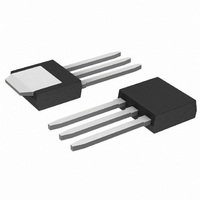
NTD3055L170-001 ON Semiconductor, NTD3055L170-001 Datasheet - Page 2

NTD3055L170-001
Manufacturer Part Number
NTD3055L170-001
Description
MOSFET N-CH 60V 9A TO-251A
Manufacturer
ON Semiconductor
Datasheet
1.NTD3055L170T4G.pdf
(8 pages)
Specifications of NTD3055L170-001
Fet Type
MOSFET N-Channel, Metal Oxide
Fet Feature
Logic Level Gate
Rds On (max) @ Id, Vgs
170 mOhm @ 4.5A, 5V
Drain To Source Voltage (vdss)
60V
Current - Continuous Drain (id) @ 25° C
9A
Vgs(th) (max) @ Id
2V @ 250µA
Gate Charge (qg) @ Vgs
10nC @ 5V
Input Capacitance (ciss) @ Vds
275pF @ 25V
Power - Max
1.5W
Mounting Type
Surface Mount
Package / Case
IPak, TO-251, DPak, VPak (3 straight leads + tab)
Lead Free Status / RoHS Status
Contains lead / RoHS non-compliant
Other names
NTD3055L170-001OS
3. Pulse Test: Pulse Width ≤ 300 ms, Duty Cycle ≤ 2%.
4. Switching characteristics are independent of operating junction temperatures.
†For information on tape and reel specifications, including part orientation and tape sizes, please refer to our Tape and Reel Packaging
ELECTRICAL CHARACTERISTICS
OFF CHARACTERISTICS
ON CHARACTERISTICS (Note 3)
DYNAMIC CHARACTERISTICS
SWITCHING CHARACTERISTICS (Note 4)
SOURCE−DRAIN DIODE CHARACTERISTICS
ORDERING INFORMATION
Specifications Brochure, BRD8011/D.
NTD3055L170G
NTD3055L170−1G
NTD3055L170T4G
Drain−to−Source Breakdown Voltage (Note 3)
Temperature Coefficient (Positive)
Zero Gate Voltage Drain Current
Gate−Body Leakage Current (V
Gate Threshold Voltage (Note 3)
Threshold Temperature Coefficient (Negative)
Static Drain−to−Source On−Resistance (Note 3)
Static Drain−to−Source On−Voltage (Note 3)
Forward Transconductance (Note 3) (V
Input Capacitance
Output Capacitance
Transfer Capacitance
Turn−On Delay Time
Rise Time
Turn−Off Delay Time
Fall Time
Gate Charge
Forward On−Voltage
Reverse Recovery Time
Reverse Recovery Stored Charge
(V
(V
(V
(V
(V
(V
(V
GS
DS
DS
DS
GS
GS
GS
= 0 Vdc, I
= 60 Vdc, V
= 60 Vdc, V
= V
= 5.0 Vdc, I
= 5.0 Vdc, I
= 5.0 Vdc, I
GS
, I
D
D
= 250 mAdc)
D
D
D
= 250 mAdc)
GS
GS
Device
= 4.5 Adc)
= 9.0 Adc)
= 4.5 Adc, T
= 0 Vdc)
= 0 Vdc, T
Characteristic
GS
J
J
= 150°C)
= ± 15 Vdc, V
= 150°C)
(I
S
(I
DS
S
= 9.0 Adc, V
(T
= 9.0 Adc, V
= 8.0 Vdc, I
(V
(V
(V
J
(I
dI
= 25°C unless otherwise noted)
DS
S
DD
DS
V
S
GS
R
= 9.0 Adc, V
/dt = 100 A/ms) (Note 3)
= 25 Vdc, V
= 30 Vdc, I
= 48 Vdc, I
DS
G
V
= 5.0 Vdc) (Note 3)
= 9.1 W) (Note 3)
f = 1.0 MHz)
GS
= 0 Vdc)
GS
D
= 5.0 Vdc,
GS
= 6.0 Adc)
= 0 Vdc, T
http://onsemi.com
= 0 Vdc) (Note 3)
GS
D
D
GS
= 9.0 Adc,
= 9.0 Adc,
= 0 Vdc,
= 0 Vdc,
(Pb−Free)
(Pb−Free)
(Pb−Free)
Package
DPAK−3
J
DPAK
DPAK
2
= 150°C)
V
Symbol
R
V
V
(BR)DSS
t
t
I
I
C
Q
DS(on)
DS(on)
C
V
GS(th)
C
g
d(on)
d(off)
DSS
GSS
Q
Q
Q
t
t
t
FS
oss
t
t
SD
rss
RR
iss
rr
a
b
r
f
T
1
2
Min
1.0
60
−
−
−
−
−
−
−
−
−
−
−
−
−
−
−
−
−
−
−
−
−
−
−
−
−
2500 Tape & Reel
75 Units/Rail
75 Units/Rail
0.031
53.6
0.98
0.85
29.8
17.6
12.2
Typ
153
195
Shipping
1.7
4.2
1.8
1.3
7.3
9.7
4.7
1.4
2.9
70
29
69
10
38
−
−
−
−
±100
†
Max
1.25
170
275
100
150
1.0
2.0
2.1
10
42
20
20
80
10
−
−
−
−
−
−
−
−
−
−
−
−
mV/°C
mV/°C
mhos
mAdc
nAdc
Unit
Vdc
Vdc
Vdc
Vdc
mW
nC
mC
pF
ns
ns


