NIF9N05CLT1 ON Semiconductor, NIF9N05CLT1 Datasheet
NIF9N05CLT1
Specifications of NIF9N05CLT1
Available stocks


Related parts for NIF9N05CLT1

NIF9N05CLT1 Summary of contents
Page 1
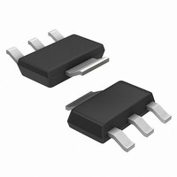
NIF9N05CL Protected Power MOSFET 2 N−Channel, Logic Level, Clamped MOSFET w/ ESD Protection in a SOT−223 Package Benefits • High Energy Capability for Inductive Loads • Low Switching Noise Generation Features • Diode Clamp Between Gate and ...
Page 2
MOSFET ELECTRICAL CHARACTERISTICS Characteristic OFF CHARACTERISTICS Drain−to−Source Breakdown Voltage (Note 1.0 mA 25° 1.0 mA −40°C to 125° ...
Page 3
MOSFET ELECTRICAL CHARACTERISTICS Characteristic SWITCHING CHARACTERISTICS (Note 4) Turn−On Delay Time Rise Time Turn−Off Delay Time Fall Time Turn−On Delay Time Rise Time Turn−Off Delay Time Fall Time Turn−On Delay Time Rise Time Turn−Off Delay Time Fall Time Gate Charge ...
Page 4
V = 10, 5 & 3 3 3 2.8 V 2 DRAIN−TO−SOURCE VOLTAGE (VOLTS) ...
Page 5
... GATE RESISTANCE (W) G Figure 9. Resistance Switching Time Variation vs. Gate Resistance ORDERING INFORMATION Device NIF9N05CLT1 NIF9N05CLT1G NIF9N05CLT3 NIF9N05CLT3G †For information on tape and reel specifications, including part orientation and tape sizes, please refer to our Tape and Reel Packaging Specifications Brochure, BRD8011/D. NIF9N05CL TYPICAL PERFORMANCE CURVES ...
Page 6
... A1 *For additional information on our Pb−Free strategy and soldering details, please download the ON Semiconductor Soldering and Mounting Techniques Reference Manual, SOLDERRM/D. ON Semiconductor and are registered trademarks of Semiconductor Components Industries, LLC (SCILLC). SCILLC reserves the right to make changes without further notice to any products herein ...