NTD20N03L27-1G ON Semiconductor, NTD20N03L27-1G Datasheet

MOSFET N-CH 30V 20A IPAK

NTD20N03L27-1G

Manufacturer Part Number
NTD20N03L27-1G
Description
MOSFET N-CH 30V 20A IPAK
Manufacturer
ON Semiconductor
Datasheet

Specifications of NTD20N03L27-1G

Fet Type
MOSFET N-Channel, Metal Oxide
Fet Feature
Logic Level Gate
Rds On (max) @ Id, Vgs
27 mOhm @ 10A, 5V
Drain To Source Voltage (vdss)
30V
Current - Continuous Drain (id) @ 25° C
20A
Vgs(th) (max) @ Id
2V @ 250µA
Gate Charge (qg) @ Vgs
18.9nC @ 10V
Input Capacitance (ciss) @ Vds
1260pF @ 25V
Power - Max
1.75W
Mounting Type
Surface Mount
Package / Case
IPak, TO-251, DPak, VPak (3 straight leads + tab)
Configuration
Single
Transistor Polarity
N-Channel
Resistance Drain-source Rds (on)
0.027 Ohms
Forward Transconductance Gfs (max / Min)
21 S
Drain-source Breakdown Voltage
30 V
Gate-source Breakdown Voltage
+/- 20 V
Continuous Drain Current
20 A
Power Dissipation
74 W
Maximum Operating Temperature
+ 150 C
Mounting Style
SMD/SMT
Minimum Operating Temperature
- 55 C
Lead Free Status / RoHS Status
Lead free / RoHS Compliant

Available stocks

Company
Part Number
Manufacturer
Quantity
Price
Part Number:
NTD20N03L27-1G
Manufacturer:
ON
Quantity:
1 946
Part Number:
NTD20N03L27-1G
Manufacturer:
ON Semiconductor
Quantity:
10
NTD20N03L27
Power MOSFET
20 Amps, 30 Volts, N−Channel DPAK
that provides the “best of design” available today in a low cost power
package. Avalanche energy issues make this part an ideal design in.
The drain−to−source diode has a ideal fast but soft recovery.
Features
Typical Applications
Stresses exceeding Maximum Ratings may damage the device. Maximum
Ratings are stress ratings only. Functional operation above the Recommended
Operating Conditions is not implied. Extended exposure to stresses above the
Recommended Operating Conditions may affect device reliability.
1. When surface mounted to an FR4 board using the minimum recommended
MAXIMUM RATINGS
© Semiconductor Components Industries, LLC, 2010
October, 2010 − Rev. 4
Drain−to−Source Voltage
Drain−to−Gate Voltage (R
Gate−to−Source Voltage
Drain Current
Total Power Dissipation @ T
Operating and Storage Temperature Range
Single Pulse Drain−to−Source Avalanche
Thermal Resistance
Maximum Lead Temperature for Soldering
Purposes, 1/8″ from case for 10 seconds
This logic level vertical power MOSFET is a general purpose part
Ultra−Low R
SPICE Parameters Available
Diode is Characterized for use in Bridge Circuits
I
High Avalanche Energy Specified
ESD JEDAC rated HBM Class 1, MM Class A, CDM Class 0
These Devices are Pb−Free and are RoHS Compliant
Power Supplies
Inductive Loads
PWM Motor Controls
Replaces MTD20N03L in many Applications
pad size and repetitive rating; pulse width limited by maximum junction
temperature.
DSS
Derate above 25°C
Energy − Starting T
(V
I
L(pk)
DD
and V
= 24 A, V
= 30 Vdc, V
− Continuous
− Non−Repetitive (t
− Continuous @ T
− Continuous @ T
− Single Pulse (t
− Junction−to−Case
− Junction−to−Ambient
− Junction−to−Ambient (Note 1)
DS(on)
DS(on)
DS
Rating
Specified at Elevated Temperatures
GS
= 34 Vdc)
, Single Base, Advanced Technology
J
(T
= 5 Vdc, L = 1.0 mH,
= 25°C
GS
C
p
v10 ms)
= 25°C unless otherwise noted)
A
A
A
C
= 1.0 MW)
p
= 25_C
= 100_C
= 25_C
v10 ms)
= 25°C (Note 1)
Symbol
T
V
V
R
R
R
V
V
J
E
I
P
DGR
, T
DSS
DM
T
I
I
qJC
qJA
qJA
GS
GS
D
D
AS
D
L
stg
−55 to
Value
"20
"24
1.75
1.67
71.4
150
288
100
260
0.6
30
30
20
16
60
74
1
W/°CW
°C/W
Unit
Vdc
Vdc
Vdc
Adc
Apk
mJ
°C
°C
W
1 2
See detailed ordering and shipping information in the package
dimensions section on page 2 of this data sheet.
1
2
3
20 A, 30 V, R
3
4
ORDERING INFORMATION
4
20N3L = Device Code
Y
WW
G
G
http://onsemi.com
CASE 369C
CASE 369D
STYLE 2
STYLE 2
DPAK−3
= Year
= Work Week
= Pb−Free Package
N−Channel
DPAK
D
DS(on)
Publication Order Number:
S
Gate
Gate
= 27 mW
DIAGRAMS
NTD20N03L27/D
MARKING
1
1
Drain
Drain
Drain
Drain
4
4
2
2
3
Source
3
Source

Related parts for NTD20N03L27-1G

NTD20N03L27-1G Summary of contents

Page 1

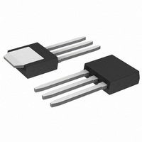
... DS(on) N−Channel MARKING DIAGRAMS 4 Drain 4 DPAK CASE 369C STYLE Drain Gate Source 4 Drain 4 DPAK−3 CASE 369D STYLE Gate Drain Source 20N3L = Device Code Y = Year WW = Work Week G = Pb−Free Package ORDERING INFORMATION Publication Order Number: NTD20N03L27/D ...

Page 2

... Pulse Test: Pulse Width ≤ 300 ms, Duty Cycle ≤ 2%. 3. Switching characteristics are independent of operating junction temperature. ORDERING INFORMATION Device NTD20N03L27G NTD20N03L27−1G NTD20N03L27T4G †For information on tape and reel specifications, including part orientation and tape sizes, please refer to our Tape and Reel Packaging Specifications Brochure, BRD8011/ 25°C unless otherwise noted) C ...

Page 3

25° 0.2 0.4 0.6 0.8 ...

Page 4

V − 200 1500 1000 500 C rss GATE−TO−SOURCE OR DRAIN−TO−SOURCE VOLTAGE (V) Figure 7. Capacitance Variation 1000 t r 100 t f ...

Page 5

... DETAIL 0.005 (0.13 *For additional information on our Pb−Free strategy and soldering details, please download the ON Semiconductor Soldering and Mounting Techniques Reference Manual, SOLDERRM/D. PACKAGE DIMENSIONS DPAK (SINGLE GAUGE) CASE 369C−01 ISSUE GAUGE L2 SEATING C PLANE PLANE DETAIL A ROTATED SOLDERING FOOTPRINT* 6.20 3 ...

Page 6

... S 0.025 0.040 0.63 1.01 V 0.035 0.050 0.89 1.27 Z 0.155 −−− 3.93 −−− STYLE 2: PIN 1. GATE 2. DRAIN 3. SOURCE 4. DRAIN ON Semiconductor Website: www.onsemi.com Order Literature: http://www.onsemi.com/orderlit For additional information, please contact your local Sales Representative NTD20N03L27/D/D ...

Related keywords